


Summary
A bifacial solar cell (BSC) is any photovoltaic solar cell that can produce electrical energy when illuminated on either of its surfaces, front or rear. In contrast, monofacial solar cells produce electrical energy only when photons impinge on their front side. Bifacial solar cells can make use of albedo radiation, which is useful for applications where a lot of light is reflected on surfaces such as roofs. The concept was introduced as a means of increasing the energy output in solar cells. Efficiency of solar cells, defined as the ratio of incident luminous power to generated electrical power under one or several suns (1 sun = 1000W/m2 [2]), is measured independently for the front and rear surfaces for bifacial solar cells. The bifaciality factor (%) is defined as the ratio of rear efficiency in relation to the front efficiency subject to the same irradiance.[3]


The vast majority of solar cells today are made of silicon (Si). Silicon is a semiconductor and as such, its external electrons are in an interval of energies called the valence band and they completely fill the energy levels of this band. Above this valence band there is a forbidden band, or band gap, of energies within which no electron can exist, and further above, we find the conduction band. The conduction band of semiconductors is almost empty of electrons, but it is where valence band electrons will find accommodation after being excited by the absorption of photons. The excited electrons have more energy than the ordinary electrons of the semiconductor. The electrical conductivity of Si, as described so far, called intrinsic silicon, is exceedingly small. Introducing impurities to the Si in the form of phosphorus atoms will provide additional electrons located in the conduction band, rendering the Si n-type, with a conductivity that can be engineered by modifying the density of phosphorus atoms. Alternatively, impurification with boron or aluminum atoms renders the Si p-type, with a conductivity that can also be engineered. These impurity atoms retrieve electrons from the valence band leaving the so-called "holes" in it, that behave like virtual positive charges.[4]
Si solar cells are usually doped with boron, so behaving as a p-type semiconductor and have a narrow (~0.5 microns) superficial n-type region. Between the p-type region and the n-type region the so-called p-n junction is formed, in which an electric field is formed which separates electrons and holes, the electrons towards the n-type region at the surface and the holes towards the p-type region. Under illumination an excess of electron-hole pairs are generated, because more electrons are excited. Thus, a photocurrent is generated, which is extracted by metal contacts located on both faces of the semiconductor. The electron-hole pairs generated by light falling outside the p-n junction are not separated by the electric field, and thus the electron-hole pairs end up recombining without producing a photocurrent.[4] The roles of the p and n regions in the cell can be interchanged. Accordingly, a monofacial solar cell produces photocurrent only if the face where the junction has been formed is illuminated. Instead, a bifacial solar cell is designed in such a way that the cell will produce a photocurrent when either side, front or rear, is illuminated.
BSCs and modules (arrays of BSCs) were invented and first produced for space and earth applications in the late 1970s, and became mainstream solar cell technology by the 2010s. It is foreseen that it will become the leading approach to photovoltaic solar cell manufacturing by 2030 due to the shown benefits over monofacial options including increased performance, versatility, and reduce soiling impact.[5]
History of the bifacial solar cell edit
Invention and first devices edit

A silicon solar cell was first patented in 1946 by Russell Ohl when working at Bell Labs and first publicly demonstrated at the same research institution by Calvin Fuller, Daryl Chapin, and Gerald Pearson in 1954; however, these first proposals were monofacial cells and not designed to have their rear face active.[6][7] The first bifacial solar cell theoretically proposed is in a Japanese patent with a priority date 4 October 1960, by Hiroshi Mori, when working for the company Hayakawa Denki Kogyo Kabushiki Kaisha (in English, Hayakawa Electric Industry Co. Ltd.), which later developed into nowadays Sharp Corporation.[8] The proposed cell was a two-junction pnp structure with contact electrodes attached to two opposite edges.
However, first demonstrations of bifacial solar cells and panels were carried out in the Soviet Space Program in the Salyut 3 (1974) and Salyut 5 (1976) LEO military space stations. These bifacial solar cells were developed and manufactured by Bordina et al. at the VNIIT (All Union Scientific Research Institute of Energy Sources) in Moscow that in 1975 became Russian solar cell manufacturer KVANT.[9] In 1974 this team filed a US patent in which the cells were proposed with the shape of mini-parallelepipeds of maximum size 1mm × 1mm × 1mm connected in series so that there were 100 cells/cm2.[10] As in modern-day BSCs, they proposed the use of isotype junctions pp+ close to one of the light-receiving surfaces. In Salyut 3, small experimental panels with a total cell surface of 24 cm2 demonstrated an increase in energy generation per satellite revolution due to Earth's albedo of up to 34%, compared to monofacial panels at the time. A 17–45% gain due to the use of bifacial panels (0.48m2 – 40W) was recorded during the flight of Salyut 5 space station.[11][12]
Simultaneous to this Russian research, on the other side of the Iron Curtain, the Laboratory of Semiconductors at the School of Telecommunication Engineering of the Technical University of Madrid, led by Professor Antonio Luque, independently carries out a broad research program seeking the development of industrially feasible bifacial solar cells. While Mori's patent and VNIIT-KVANT spaceship-borne prototypes were based on tiny cells without surface metal grid and therefore intricately interconnected, more in the style of microelectronic devices which were at that time in their onset, Luque will file two Spanish patents in 1976 and 1977 and one in the United States in 1977 that were precursory of modern bifacials .[13][14][15]
Luque's patents were the first to propose BSCs with one cell per silicon wafer, as was by then the case of monofacial cells and so continues to be, with metal grids on both surfaces.[16] They considered both the npp+ structure and the pnp structures. Development of BSCs at the Laboratory of Semiconductors was tackled in a three-fold approach that resulted in three PhD theses, authored by Andrés Cuevas (1980), Javier Eguren (1981) and Jesús Sangrador (1982), the first two having Luque as doctoral advisor while Dr. Gabriel Sala, from the same group, conducted the third. Cuevas' thesis consisted of constructing the first of Luque's patents, the one of 1976, that due to its npn structure similar to that of a transistor, was dubbed the "transcell".[17] Eguren's thesis dealt with the demonstration of Luque's 2nd patent of 1977, with a npp+ doping profile, with the pp+ isotype junction next to the cell's rear surface, creating what is usually referred as a back surface field (BSF) in solar cell technology. This work gave way to several publications and additional patents.[18][19][20][21]
In particular, the beneficial effect of reducing p-doping in the base, where reduction of voltage in the emitter junction (front p-n junction) was compensated by voltage increase in the rear isotype junction, while at the same time enabling higher diffusion length of minority carriers that increases the current output under bifacial illumination.[22][23] Sangrador's thesis and third development route at the Technical University of Madrid, proposed the so-called vertical multijunction edge-illuminated solar cell in which p+nn+ where stacked and connected in series and illuminated by their edges, this being high voltage cells that required no surface metal grid to extract the current.[24] In 1979 the Laboratory for Semiconductors became the Institute for Solar Energy (IES-UPM), that having Luque as the first director, continued intense research on bifacial solar cells well until the first decade of the 21st century, with remarkable results. For example, in 1994, two Brazilian PhD students at the Institute of Solar Energy, Adriano Moehlecke and Izete Zanesco, together with Luque, developed and produced a bifacial solar cell rendering 18.1% in the front face and 19.1% in the rear face; a record bifaciality of 103% (at that time record efficiency for monofacial cells was slightly below 22%).[25]
-
 First page of Mori's1966 patent. In Fig. 1. p-layers (2-2') diffused on three sides of a bulk n-type silicon (1). Electrodes on both edges connect the p (4) and n (3) regions to the electric circuit. In Fig. 3. the cells are connected in series.
 -
 Drawing in Bordina's 1976 patent. Millimetric parallelipedic bifacial solar cells connected in series. In each mini-cell bulk material is p-type. Dashed lines are pn junctions and dotted lines isotype pp+. Diagonally striped lines left to right are metal electrodes and diagonally striped lines right to left is an insulator filler. 100 cells/cm2.
 -
![Drawings in Luque's 1978 patent ES458514A1 of the npp+ cell bifacial solar cell. (a): n-type layer; (b):metal grids; (c): p+-type layer; (d) p-type wafer]]](//upload.wikimedia.org/wikipedia/commons/thumb/3/30/Luque%27s_patent_of_the_npp%2B_bifacial_solar_cell.jpg/261px-Luque%27s_patent_of_the_npp%2B_bifacial_solar_cell.jpg) Drawings in Luque's 1978 patent ES458514A1 of the npp+ cell bifacial solar cell. (a): n-type layer; (b):metal grids; (c): p+-type layer; (d) p-type wafer]]
Drawings in Luque's 1978 patent ES458514A1 of the npp+ cell bifacial solar cell. (a): n-type layer; (b):metal grids; (c): p+-type layer; (d) p-type wafer]]


![Drawings in Luque's 1978 patent ES458514A1 of the npp+ cell bifacial solar cell. (a): n-type layer; (b):metal grids; (c): p+-type layer; (d) p-type wafer]]](http://upload.wikimedia.org/wikipedia/commons/thumb/3/30/Luque%27s_patent_of_the_npp%2B_bifacial_solar_cell.jpg/261px-Luque%27s_patent_of_the_npp%2B_bifacial_solar_cell.jpg)
The first bifacial solar cell factory: Isofoton edit

Of the three BSC development approaches carried out at the Institute of Solar Energy, it was that of Eguren's thesis, the npp+, the one that gave the best results. On the other hand, it was found that bifacial solar cells could deliver up to 59% more power yearly when installed with a white surface at their back, which enhanced the sun's reflected radiation (albedo radiation) going into the cells' rear face.[26][27] It could have been expected this finding to happen easier in Spain, where houses, especially rural ones are, in the south, frequently whitewashed. Hence, a spin-off company was founded to manufacture bifacial solar cells and modules, based on the npp+ development, to commercially exploit their enhanced power production when suitably installed with high albedo surfaces behind, whether ground or walls.[28][29]
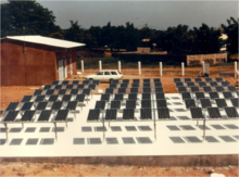
Founded in 1981 it was named Isofotón (because its cells singularly used all isotropic photons) and established in Málaga, Luque's hometown. Its initial capital came from family and friends (e.g. most of the employees and research staff of the Institute of Solar Energy) plus some public capital from an industrial development fund, SODIAN, owned by the Andalusian Autonomous Community. It set sail with 45 shareholders, Luque as 1st chairman and co-CEO, together with his brother Alberto, a seasoned industrial entrepreneur, and having Javier Eguren as CTO. Eguren and Sala led the technology transfer from the Institute of Solar Energy to Isofoton. By 1983 Isofoton's factory in Málaga had a manufacturing capacity of 330 kW/yr. of bifacial modules (with a 15 people net headcount) at a time when the global market of photovoltaics was in the range of 15 MW. At that time, the market of terrestrial photovoltaic power plants, to which Isofoton oriented its production, essentially consisted of demonstration projects.[30] Thus, early landmarks of Isofoton's production were the 20kWp power plant in San Agustín de Guadalix, built in 1986 for Iberdrola, and an off-grid installation by 1988 also of 20kWp in the village of Noto Gouye Diama (Senegal) funded by the Spanish international aid and cooperation programs.
As Isofotón matured, its early shareholding structure of individuals was replaced by big technology and engineering corporations as Abengoa or Alcatel or banks such as BBVA. Upon Alcatel's entry as a major shareholder in 1987 the decision was taken to switch production to more conventional monofacial photovoltaic cells, based on licensed technology from US PV manufacturer Arco Solar, this being the end of Isofoton as the world's first and until then, only bifacial cell manufacturer. However, Isofoton still continued to forge ahead successfully and between 2000 and 2005 it ranked consistently among the world's top 10 photovoltaic manufacturers. In 2015 it filed for bankruptcy when, as almost all of the other European and Western PV manufacturers of its time, it could not withstand the competitive pressure of the new wave of Chinese PV manufacturers.
Later progress until mass production edit

Besides Isofoton, some other PV manufacturers, however, specialized in space applications, reported developments of BSCs at a laboratory scale such as COMSAT in 1980, Solarex in 1981 or AEG Telefunken in 1984.[31][32][33] During the late 1980s and the 1990s research and improvement of bifacial solar cell technology continued. In 1987 Jaeger and Hezel at ISFH (Institute for Solar Energy Research in Hamelin) successfully produced a new BSC design based on a single junction n+p, in which the rear contact was replaced by a metal grid and all intermetallic surfaces were passivated with PECVD-grown silicon nitride, this resulting in 15% and 13.2% under front and rear illumination respectively.[34] In this way, these devices presented a Metal Insulator Semiconductor-Inversion Layer (MIS-IL) front junction. Ten years later, the same research group replaced this MIS layer with a diffused pn junction to produce BSC laboratory devices with 20.1% front and 17.2% rear efficiencies.[35] In 1997, Glunz et al., at the Fraunhofer Institute for Solar Energy Systems, produced n+pn+ 4 cm2 devices with 20.6% front and 20.2% rear conversion efficiencies.[36] This was a double junction cell (one of the junctions not connected or "floating") with the metal grid only on the rear surface, i.e. operating an interdigitated back contact (IBC) solar BSC and with the floating front junction performing as passivation. By 1997, SunPower, by then the solar cell manufacturer producing the highest efficiency cells through its back contact design, published research by a team led by its founder, Richard Swanson, on a back contact BSC with front efficiency of 21.9% and rear efficiency of 13.9%.[37] A prototype series of cells and modules were produced but never made it to mass production.
During these days, with PV module cost being almost the only driver towards a wider embracement of solar electricity – as has happened ever after – and despite their attractiveness and the large research effort carried out, the added complexity of BSCs precluded its adoption for large-scale production as had only previously been achieved by Isofoton. Niche applications where BSCs presented competitive advantages were proposed and demonstrated, even to the point of involving some pilot productions. For example, sun shading bifacial PV modules in facades or carports.[38] A celebrated application demonstration was the one by Nordmann et al. in 1997, consisting of a 10 kW PV noise barrier along a north-south-oriented 120m tranche of the A1 motorway in Wallisellen (north of Zurich). BSC cells here were manufactured by German companies ASE (later RWE Schott Solar GmbH) and Kohlhauer based on a system patent by TNC Energie Consulting, and this application has since been abundantly replicated.[39]
With the turn of the millennium, paths towards the industrial production of BSC cells and modules started to be laid again. In 2000, Japanese manufacturer Hitachi released results of its research in BSCs with another transistor-like n+pn+ cell with 21.3% front and 19.8% rear efficiency.[40] By 2003 Hitachi had developed BSC module technology that was licensed in 2006 to the US company Prism Solar.[41] In 2004 a team led by Prof. Andrew Blakers at the Australian National University published its first results on the so-called Sliver BSC technology, that had taken the design route previously proposed by Mori and also realized by IES-UPM by Sangrador and Sala, i.e., a stack of laterally connected bifacial cells requiring no metal grids, however, by then with more advanced means with which thousands of cells were micromachined out of one p-type silicon wafer.[42][43] The technology was later transferred to Origin Energy that planned large-scale manufacturing for the Australian market by 2008, but finally this never occurred due to price pressure from Chinese competition.[44] In 2012 Sanyo (later acquired by Panasonic) successfully launches industrial production of bifacial PV modules, based on its HIT (Heterojunction with Intrinsic Thin layer) technology.[45][46] By 2010, ECN releases results on its research on BSCs, based on the by then classical p+nn+ Back Surface Field BSC.[47] This technology, dubbed n-PASHA, was transferred to the leading Chinese PV manufacturer Yingli by 2012, that began to commercialize them under the brand name Panda.[48] Yingli was at that time the no.1 PV producer holding 10% of the world's shipments, and this technology transfer by ECN can be considered a milestone in the ultimate coming of age of BSCs, in which the technology is picked up by the, by then, mighty Chinese manufacturers mainly responsible for the steep decrease experienced PV prices since the beginning of the 2010s.
By 2020, the ENF Solar directory of solar companies lists 184 producers of bifacial solar panels, and according to the International Technology Roadmap for Photovoltaics, they held a 20% share of the overall PV market and its forecast is that this share will rise to 70% by 2030. When looking back on the development history of the BSC, it seems clear that fully industrializing the monofacial PV solar cells and the development of its nowadays booming market, was a necessary condition for BSCs to become a next step in the advancement of PV solar cell technology, with a solar market and industry that can thus make the most of its performance advantages.
Current bifacial solar cells edit


Several in-depth reviews on bifacial solar cells and their technology elements cover the current state-of-the-art. They summarize the most common BSC designs currently being marketed and then provide a review of their technological aspects.[49][50][3]
BSC types in the market edit
Various bifacial PV modules with different architectures for their BSCs are currently available in the PV market. These include Passivated Emitter Rear Contact (PERC), Passivated Emitter Rear Locally-diffused (PERL), Passivated Emitter Rear Totally diffused (PERT), Heterojunction with Intrinsic Thin-layer (HIT), Interdigitated Back Contact (IBC).
PERT edit
- Efficiency: 19.5–22% (front), 17–19% (rear)
- Bifaciality: 80–90%
- Mostly commercialized (e.g. Yingli, Trina, LG) on the n-type c-Si wafer due to longer carrier lifetime than p-type and absence of boron in the bulk material avoiding light induced degradation (LID).
PERL edit
- Efficiency: 19.8% (front)
- Bifaciality: 80–90%
- Mainly based on p-type c-Si wafer
- Boron is locally diffused into contact areas at the rear side
PERC edit
- Efficiency: 19.4–21.2% (front), 16.7–18.1% (rear)
- Bifaciality: 70–80%
- Mostly commercialized (e.g. JA Solar, LONGi, Trina) e.g. on the p-type c-Si wafer
IBC edit
- Efficiency: 23.2%
- Bifaciality: 70–80%
- Mainly based on n-type c-Si wafer
- No metal grid contact on the front side
HIT edit
- Efficiency: 24.7%
- Bifaciality: 95–100%
- Mostly commercialized (e.g. Panasonic, Hanergy) on n-type c-Si wafer
Technology aspects edit
Silicon wafers have traditionally been used as cell substrates, although other materials have been proposed and proven. The thickness of the substrate has an essential impact on material costs; thinner wafers mean savings, but at the same time, they make handling more difficult and costly or impact the throughput. Also, thinner substrates can improve efficiency due to the reduction of bulk recombination.[51]
While monofacial cells require only one diffusion step when forming their single p-n junction, BSCs require two p-n junctions with different dopants which increase the number of high temperature processes in the manufacturing and, therefore its cost. Co-diffusion is one option to simplify this process, consisting in the pre-deposition and doping of boron and phosphorus on both sides of the cell simultaneously; however, it requires controlling there will be no cross-doping. Another cost-saving option is to build the p-n junctions using ion implantation instead of diffusion.
As in monofacial cells, front contacts in BSCs cells are mainly silver screen printed that become, due to the silver content, one of its important cost elements. Research is conducted to replace screen printed silver contacts with copper-plated contacts, TCOs, or aluminum. However, the most feasible so far has been to reduce the amount of screen printing paste by using front busbar-less solar cells with very thin contact wires.
In BSCs recombination at the metal-semiconductor interface in the rear surface is reduced when compared to monofacial cells, due to the former restricting this interface to that of the rear surface metal grid. However, passivation of silicon surfaces is still needed and its area extended by that of the rear surface. Again the target is to reduce the temperature of the manufacturing processes involved. Traditionally passivation was obtained by thermal oxidation (SiO2); however, this requires over 1000C temperature. Currently, silicon surface passivation is achieved by putting silicon nitride (SiNx) on both sides of the cell by means of plasma-enhanced chemical vapor deposition (PECVD), which requires 400C. Lower deposition temperatures of ~225C can be achieved by passivating with hydrogenated amorphous silicon, a-Si:H.
Bifacial solar cell performance parameters edit
The efficiency of BSCs is usually determined by means of independent efficiency measurements of the front and rear sides under one sun. Sometimes, the BSC is characterized using its equivalent efficiency, defined as the efficiency of a monofacial cell able to render the same power per unit area as the bifacial cell at the same test conditions. Alternatively, the equivalent efficiency has been defined as the sum of the front and rear side efficiencies weighted by the relative amounts of irradiance on both sides.
Another related parameter is the Bifaciality Factor, defined as the ratio of the front and rear efficiencies when illuminated and measured independently:[3]
![{\displaystyle {\text{Bifaciality factor }}(\%)=\left[{\frac {\eta _{\text{front}}}{\eta _{\text{rear}}}}\right]\times 100}](https://wikimedia.org/api/rest_v1/media/math/render/svg/a326a2239847d9b5e8a84cea1698e9e5c36a015e)
Also specific to BSCs is the Separation Rate, that intends to measure the Bifacial Illumination Effect predicted by McIntosh et al. in 1997 by which, the electrical output of BSCs operating under bifacial illumination would not necessarily equal the sum of the front-only and rear-only electrical output, i.e. it is not merely a linear combination of the monofacial characteristics:[52][53]
![{\displaystyle {\text{Separation rate }}(\%)=\left[{\frac {X_{\text{front+rear}}}{X_{\text{front}}+X_{\text{rear}}}}\right]\times 100}](https://wikimedia.org/api/rest_v1/media/math/render/svg/6d677b5f87bfdc69bec131063f9cbd10da0db8d1)
Typically X represents one of the cell characteristic parameters such as the short circuit current Jsc, the peak power Pmax or the efficiency η. Furthermore, to characterize BSC operation under simultaneous front and rear irradiation, the irradiance gain, g, defined as:[3]
so that


and a bifacial 1.x Efficiency can be defined as the efficiency obtained under a simultaneous irradiance of a certain amount on the front face and x times this amount on the rear side of the BSC. Then the actual gain of a BSC with respect to a monofacial one can be expressed through the Gain-Efficiency Product, which is the product of the irradiance gain g and the bifacial 1.x Efficiency.
References edit
- ^ "Vertical solar panels could save farm land and transform agriculture". 10 February 2023.
- ^ "Solar simulator", Wikipedia, 22 July 2023, retrieved 16 October 2023
- ^ a b c d Guerrero-Lemus, R.; Vega, R.; Kim, T.; Kimm, A.; Shephard, L.E. (2016). "Bifacial solar photovoltaics – A technology review". Renewable and Sustainable Energy Reviews. 60 (60): 1533–1549. doi:10.1016/j.rser.2016.03.041.
- ^ a b Green, Martin A. (December 1998). Solar Cells: Operating Principles, Technology and System Applications. The University of New South Wales. ISBN 0-85823-580-3.
- ^ Grau-Luque, Enric; Antonanzas-Torres, Fernando; Escobar, Rodrigo (15 October 2018). "Effect of soiling in bifacial PV modules and cleaning schedule optimization". Energy Conversion and Management. 174: 615–625. Bibcode:2018ECM...174..615L. doi:10.1016/j.enconman.2018.08.065. ISSN 0196-8904. S2CID 105381395.
- ^ US 2402662A Russell Ohl / Bell Telephone Laboratories: "Light-sensitive electric device" filing date 27 May 1941
- ^ Chapin, D.M.; Fuller, C.S.; Pearson, G.L. (1954). "A new silicon p-n junction photocell for converting solar radiation into electrical power". Journal of Applied Physics. 25 (5): 676–677. Bibcode:1954JAP....25..676C. doi:10.1063/1.1721711.
- ^ US 3278811 Hiroshi Mori / Hayakawa Denki Kogyo KK: "Radiation energy transducing device" filing date 3 October 1961
- ^ Bordina, N.M.; Golovner, T.M.; Zadde, V.V.; Zaitseva, K.N.; Landsman, A.P.; Streltsova, V.I. (1975). "Operation of a thin silicon photoconverter under illumination on both sides". Applied Solar Energy. 11 (5–6): 81–86. Bibcode:1975ApSE...11...81B.
- ^ US 3948682 Ninel Mineevna Bordina, Vitaly Viktorovich Zadde, Aita Konstantinovna Zaitseva, Pavlovich Landsman, Dmitry Semenovich Strebkov, Valentina Ivanovna Streltsova, Vadim Alexeevich Unishkov: "Semiconductor Photovoltaic Generator" filing date 31 October 1974
- ^ Grigorieva, G.M.; Kagan, M.B.; Zviagina, K.N.; Kulicauscas, V.; Kreinin, L.; Bordina, N.; Eisenberg, N. (1–5 September 2008). "Future of Bifacial Si Solar Cells for Space Application". 23rd European Photovoltaic Solar Energy Conference, Valencia, Spain.
- ^ Letin, V.A.; Kagan, M.B.; Nadorov, V.P.; Zayavlin, V.R. (2003). "Bifacial Solar Arrays of Russian Space Crafts". Geliotekhnika. 1.
- ^ ES 453575A1 Antonio Luque "Procedimiento para la conversion de energia solar y dispositive para la puesta en practica de este procedimiento" filing date 24 November 1976
- ^ ES 458514A1 Antonio Luque "Procedimiento para obtener celulas solare bifaciales" filing date 5 May 1977
- ^ US 4169738 Antonio Luque "Double-sided solar cell with self-refrigerating concentrator" filing date 21 November 1977
- ^ Luque, A.; Ruiz, J.M.; Cuevas, A.; Eguren, J.; Gómez-Agost, J.M. (1977). "Double-sided solar cells to improve static concentration". Proceedings of the 1st. European Conference on Photovoltaic Solar Energy: 269–277.
- ^ Luque, A.; Cuevas, A.; Ruiz, J.M. (1980). "Double-sided n+-p-n+ solar cell for bifacial concentration". Solar Cells. 2 (2): 151–166. doi:10.1016/0379-6787(80)90007-1.
- ^ Luque, A.; Cuevas, A.; Eguren, J. (1978). "Solar cell behaviour under variable surface recombination velocity and proposal of a novel structure". Solid State Electronics. 21 (5): 793–794. Bibcode:1978SSEle..21..793L. doi:10.1016/0038-1101(78)90014-X.
- ^ Luque, A.; Eguren, J.; del Alamo, J. (1978). "Internal quantum efficiency of back-illuminated n+pp+ solar cells". Revue de Physique Appliquée. 13 (12): 629. doi:10.1051/rphysap:019780013012062900.
- ^ Eguren, J.; Del Alamo, J.; Luque, A. (1980). "Optimization of p+ doping level n+-p-p+ bifacial solar cells by ion implantatation". Electronics Letters. 16 (16): 633–634. doi:10.1049/el:19800439.
- ^ Cuevas, A.; Luque, A.; Eguren, J.; del Alamo, J. (1981). "High efficiency bifacial back surface field solar cells". Solar Cells. 3 (4): 337–340. Bibcode:1981SoCe....3..337C. doi:10.1016/0379-6787(81)90024-7.
- ^ Luque, A.; Eguren, J (1982). "High injection phenomena in p+-i-n+ silicon solar cells". Solid State Electronics. 25 (8): 797–809. Bibcode:1982SSEle..25..797L. doi:10.1016/0038-1101(82)90210-6.
- ^ Eguren, J.; del Alamo, J.; Cuevas, A.; Luque, A. (1981). "High Efficiency p+nn+ bifacial solar cells". Fifteenth IEEE Photovoltaic Specialists Conference: 1343–1348.
- ^ Sangrador, J.; Sala, G. (1979). Two- dimensional analysis of the collection efficiency of vertical multijunction solar cells. 1979 International Electron Devices Meeting. pp. 318–321. doi:10.1109/IEDM.1979.189613. S2CID 26189505.
- ^ Moehlecke, A.; Zanesco, I.; Luque, A. (1994). "Practical high efficiency bifacial solar cells". Proceedings of 1994 IEEE 1st World Conference on Photovoltaic Energy Conversion - WCPEC (A Joint Conference of PVSC, PVSEC and PSEC). Vol. 2. pp. 1663–1666. doi:10.1109/WCPEC.1994.520538. ISBN 0-7803-1460-3. S2CID 137189024.
- ^ Cuevas, A.; Luque, A.; Eguren, J.; del Alamo, J. (1982). "50% more output power from an albedo-collecting flat panel using bifacial solar cells". Solar Energy. 19: 419–420. doi:10.1016/0038-092X(82)90078-0.
- ^ Luque, A.; Lorenzo, E.; Sala, G.; Lopez-Romero, S. (1984). "Diffusing reflectors for bifacial photovoltaic panels". Solar Cells. 13 (3): 277–292. doi:10.1016/0379-6787(85)90021-3.
- ^ Eguren, Javier; Martínez-Moreno, Francisco; Merodio, Pablo; Lorenzo, Eduardo (2022). "First bifacial PV modules early 1983". Solar Energy. 243: 327–335. Bibcode:2022SoEn..243..327E. doi:10.1016/j.solener.2022.08.002. ISSN 0038-092X. S2CID 251552073.
- ^ Lorenzo, Eduardo (2021). "On the historical origins of bifacial PV modelling". Solar Energy. 218: 587–595. Bibcode:2021SoEn..218..587L. doi:10.1016/j.solener.2021.03.006. S2CID 233573242.
- ^ Mints, Paula (April 2017). "Photovoltaic Manufacturer Capacity, Shipments, Price & Revenues 2016/2017". SPV Market Research. 5.
- ^ Meulenberg, A.; Allison, J.F.; Arndt, R.A. (1980). "Thin n-i-p silicon solar cell". Proceedings of the 14th IEEE Photovoltaic Specialists Conference, San Diego: 161–165. Bibcode:1980pvsp.conf..161M.
- ^ Giuliano, M.; Wohlgemuth, J. (1981). "The grided back contact and its effect on solar cell performance". Proceedings of the IEEE Photovoltaic Specialists Conference, Kissimmee: 111–114.
- ^ Strobl, G.; Kasper, C.; Rasch, K.D.; Roy, K. (1985). "Bifacial space silicon solar cell". Proceedings of the 18th IEEE Photovoltaic Specialists Conference, Las Vegas: 454–457. Bibcode:1985pvsp.conf..454S.
- ^ Jaeger, K.; Hezel, R. (1987). "Bifacial MIS inversion layer solar cells based on low temperature silicon surface passivation". Proceedings of the 19th IEEE Photovoltaic Specialists Conference, New Orleans: 388–391. Bibcode:1987pvsp.conf..388J.
- ^ Hubner, A.; Aberle, A.; Hezel, R. (1997). "20% efficient bifacial silicon solar cells". Proceedings of the 14th European Photovoltaic Solar Energy Conference, Barcelona, Spain: 92–95.
- ^ Glunz, S.W.; Knobloch, J.; Biro, D.; Wetting, W. (1997). "Optimized high-efficiency silicon solar cells" (PDF). Proceedings of the 14th European Photovoltaic Solar Energy Conference, Barcelona: 392–395.
- ^ Zhou, C.Z.; Verlinden, P.J.; Crane, R.A.; Swanson, R.M.; Sinton, R.A. (1997). "21.9% efficient silicon bifacial solar cells". Conference Record of the Twenty Sixth IEEE Photovoltaic Specialists Conference - 1997. pp. 287–290. doi:10.1109/PVSC.1997.654085. ISBN 0-7803-3767-0. S2CID 122824198.
- ^ Hezel, Rudolf (2003). "Novel Applications of Bifacial Solar Cells". Progress in Photovoltaics. 11 (8): 549–556. doi:10.1002/pip.510. S2CID 98393113.
- ^ Nordmann, Th.; Reiche, K.; Kleiss, G.; Frölich, A.; Goetzberger, A. (1998). "Integrated PV noise barriers: six innovative facilities, a German/Swiss technological and economical success story". Proceedings of the 2nd World Conference of Photovoltaic Solar Energy Conversion, Vienna: 2486–2491.
- ^ Ohtsuka, H.; Sakamoto, M.; Tsutsui, K.; Yazawa, Y. (2000). "Bifacial silicon solar cells with 21.3% front efficiency and 19.8% rear efficiency". Progress in Photovoltaics. 8 (4): 385–390. doi:10.1002/1099-159X(200007/08)8:4<385::AID-PIP340>3.0.CO;2-B.
- ^ Uematsu, T.; Tsutsui, K.; Yazawa, Y.; Warabisako, T.; Araki, I.; Eguchi, Y.; Joge, T. (2003). "Development of bifacial PV cells for new applications of flat-plate modules". Solar Energy Materials and Solar Cells. 75 (3–4): 557–566. doi:10.1016/S0927-0248(02)00197-6.
- ^ Blakers, A.W.; Stocks, M.J.; Weber, K.J.; Everett, V.; Babaei, J.; Verlinden, P.; Kerr, M.; Stuckings, M.; Mackey, P. (2003). "Sliver Solar Cells". 13th NREL Workshop on Crystalline Si Materials and Processing, Vail.
- ^ Weber, K.J.; Blakers, A.W.; Stocks, M.J.; Babaei, J.H.; Everett, V.A.; Neuendorf, A.J.; Verlinden, P. (2004). "A Novel Low Cost, High Efficiency Micromachined Silicon Solar Cell". Electron Device Letters. 25 (1): 37–39. Bibcode:2004IEDL...25...37W. doi:10.1109/LED.2003.821600. S2CID 21606033.
- ^ Vorath, Sophia (30 May 2012). "Origin Energy closes Sliver solar factory, flags writedown". Renew Economy. Retrieved 25 October 2020.
- ^ Mishima, Takahiro; Taguchi, Mikio; Sakata, Hitoshi; Marujama, Eiji (2011). "Development status of high-efficiency HIT solar cells". Solar Energy Materials and Solar Cells. 95 (1): 18–21. doi:10.1016/j.solmat.2010.04.030.
- ^ a%20high%20power%20generation%20capacity. "Panasonic Brings its HIT Double Solar Modules to the Global Market". Panasonic. 4 July 2012. Retrieved 25 October 2020.
{{cite web}}: Check|url=value (help) - ^ Burgers, A.R.; Naber, R.C.G.; Carr, A.J.; Barton, P.C.; Geerligs, L.J.; Jingfeng, X.; Gaofei, L.; Weipeng, S.; Haijiao, A.; Venema, P.R.; Vlooswijk, A.H.G (2010). "19% efficient n-type Si solar cells made in pilot production". 25th European Photovoltaic Solar Energy Conference, Valencia, Spain: 1106–1109.
- ^ Romijn, I.G.; van Aken, B.; Anker, J.; Burgers, A.R.; Heurtault, B.; Koppes, M.; Kossen, E.; Lamers, M.; Saynova, D.S.; Tool, C.J.J.; Fang, L.; Jingfeng, X.; Gaofei, L.; Zhuo, X.; Hongfang, W.; Zhiyan, H.; Venema, P.R.; Vlooswijk, A.H.G. (2012). "Industrial implementation of efficiency improvements in n-type solar cells and modules". Proceedings of the 22nd International Photovoltaic Science and Engineering Conference, Hangzhou.
- ^ Liang, T.S.; Pravettoni, M.; Deline, C.; Stein, J.S.; Kopecek, R.; Singh, J.P. (2019). "A review of crystalline silicon bifacial photovoltaic performance characterisation and simulation". Energy & Environmental Science. 143: 1285–1298.
- ^ Gu, Wenbo; Ma, Tao; Ahmed, Salman; Zang, Yijie; Peng, Jinqing (2020). "A comprehensive review and outlook of bifacial photovoltaic (bPV) technology". Energy Conversion and Management. 223 (223): 113283. Bibcode:2020ECM...22313283G. doi:10.1016/j.enconman.2020.113283. S2CID 224867963.
- ^ Pan, A.; del Cañizo, C.; Luque, A. (2007). "Effect of thickness on bifacial silicon solar cells". 2007 Spanish Conference on Electron Devices. pp. 234–237. doi:10.1109/SCED.2007.384035. ISBN 978-1-4244-0868-9. S2CID 43201133.
- ^ Ohtsuka, H.; Sakamoto, M.; Koyama, M.; Tsutsui, K.; Uematsu, T.; Yazawa, Y. (2001). "Characteristics of Bifacial Solar Cells Under Bifacial Illumination with Various Intensity Levels". Progress in Photovoltaics. 9: 1–13. doi:10.1002/pip.336. S2CID 98812151.
- ^ McIntosh, K.R.; Honsberg, C.B.; Wenham, S.R. (1998). "The impact of rear illumination on bifacial solar cells with ¯oating junction passivation". Proceedings of the 2nd World Conference and Exhibition on Photovoltaic Solar Energy Conversion, Vienna: 1515–1518.