


Summary
Electron-beam lithography (often abbreviated as e-beam lithography or EBL) is the practice of scanning a focused beam of electrons to draw custom shapes on a surface covered with an electron-sensitive film called a resist (exposing).[1] The electron beam changes the solubility of the resist, enabling selective removal of either the exposed or non-exposed regions of the resist by immersing it in a solvent (developing). The purpose, as with photolithography, is to create very small structures in the resist that can subsequently be transferred to the substrate material, often by etching.
The primary advantage of electron-beam lithography is that it can draw custom patterns (direct-write) with sub-10 nm resolution. This form of maskless lithography has high resolution but low throughput, limiting its usage to photomask fabrication, low-volume production of semiconductor devices, and research and development.
Systems edit
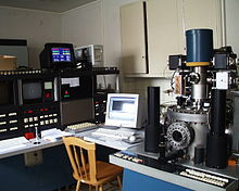
Electron-beam lithography systems used in commercial applications are dedicated e-beam writing systems that are very expensive (> US$1M). For research applications, it is very common to convert an electron microscope into an electron beam lithography system using relatively low cost accessories (< US$100K). Such converted systems have produced linewidths of ~20 nm since at least 1990, while current dedicated systems have produced linewidths on the order of 10 nm or smaller.
Electron-beam lithography systems can be classified according to both beam shape and beam deflection strategy. Older systems used Gaussian-shaped beams that scanned these beams in a raster fashion. Newer systems use shaped beams that can be deflected to various positions in the writing field (also known as vector scan).
Electron sources edit
Lower-resolution systems can use thermionic sources (cathode), which are usually formed from lanthanum hexaboride. However, systems with higher-resolution requirements need to use field electron emission sources, such as heated W/ZrO2 for lower energy spread and enhanced brightness. Thermal field emission sources are preferred over cold emission sources, in spite of the former's slightly larger beam size, because they offer better stability over typical writing times of several hours.
Lenses edit
Both electrostatic and magnetic lenses may be used. However, electrostatic lenses have more aberrations and so are not used for fine focusing. There is currently[when?] no mechanism to make achromatic electron beam lenses, so extremely narrow dispersions of the electron beam energy are needed for finest focusing.[citation needed][needs update]
Stage, stitching and alignment edit

Typically, for very small beam deflections, electrostatic deflection "lenses" are used; larger beam deflections require electromagnetic scanning. Because of the inaccuracy and because of the finite number of steps in the exposure grid, the writing field is of the order of 100 micrometre – 1 mm. Larger patterns require stage moves. An accurate stage is critical for stitching (tiling writing fields exactly against each other) and pattern overlay (aligning a pattern to a previously made one).
Electron beam write time edit
The minimum time to expose a given area for a given dose is given by the following formula:[2]

where is the time to expose the object (can be divided into exposure time/step size), is the beam current, is the dose and is the area exposed.


For example, assuming an exposure area of 1 cm2, a dose of 10−3 coulombs/cm2, and a beam current of 10−9 amperes, the resulting minimum write time would be 106 seconds (about 12 days). This minimum write time does not include time for the stage to move back and forth, as well as time for the beam to be blanked (blocked from the wafer during deflection), as well as time for other possible beam corrections and adjustments in the middle of writing. To cover the 700 cm2 surface area of a 300 mm silicon wafer, the minimum write time would extend to 7*108 seconds, about 22 years. This is a factor of about 10 million times slower than current optical lithography tools. It is clear that throughput is a serious limitation for electron beam lithography, especially when writing dense patterns over a large area.
E-beam lithography is not suitable for high-volume manufacturing because of its limited throughput. The smaller field of electron beam writing makes for very slow pattern generation compared with photolithography (the current standard) because more exposure fields must be scanned to form the final pattern area (≤mm2 for electron beam vs. ≥40 mm2 for an optical mask projection scanner). The stage moves in between field scans. The electron beam field is small enough that a rastering or serpentine stage motion is needed to pattern a 26 mm X 33 mm area for example, whereas in a photolithography scanner only a one-dimensional motion of a 26 mm X 2 mm slit field would be required.
Currently an optical maskless lithography tool[3] is much faster than an electron beam tool used at the same resolution for photomask patterning.
Shot noise edit
As features sizes shrink, the number of incident electrons at fixed dose also shrinks. As soon as the number reaches ~10000, shot noise effects become predominant, leading to substantial natural dose variation within a large feature population. With each successive process node, as the feature area is halved, the minimum dose must double to maintain the same noise level. Consequently, the tool throughput would be halved with each successive process node.
| feature diameter (nm) | minimum dose for one-in-a-million 5% dose error (μC/cm2) |
|---|---|
| 40 | 127 |
| 28 | 260 |
| 20 | 509 |
| 14 | 1039 |
| 10 | 2037 |
| 7 | 4158 |
Note: 1 ppm of population is about 5 standard deviations away from the mean dose.
Ref.: SPIE Proc. 8683-36 (2013)
Shot noise is a significant consideration even for mask fabrication. For example, a commercial mask e-beam resist like FEP-171 would use doses less than 10 μC/cm2,[4][5] whereas this leads to noticeable shot noise for a target critical dimension (CD) even on the order of ~200 nm on the mask.[6][7] CD variation can be on the order of 15–20% for sub-20 nm features.[8][9]
Defects in electron-beam lithography edit
Despite the high resolution of electron-beam lithography, the generation of defects during electron-beam lithography is often not considered by users. Defects may be classified into two categories: data-related defects, and physical defects.
Data-related defects may be classified further into two sub-categories. Blanking or deflection errors occur when the electron beam is not deflected properly when it is supposed to, while shaping errors occur in variable-shaped beam systems when the wrong shape is projected onto the sample. These errors can originate either from the electron optical control hardware or the input data that was taped out. As might be expected, larger data files are more susceptible to data-related defects.
Physical defects are more varied, and can include sample charging (either negative or positive), backscattering calculation errors, dose errors, fogging (long-range reflection of backscattered electrons), outgassing, contamination, beam drift and particles. Since the write time for electron beam lithography can easily exceed a day, "randomly occurring" defects are more likely to occur. Here again, larger data files can present more opportunities for defects.
Photomask defects largely originate during the electron beam lithography used for pattern definition.
Electron energy deposition in matter edit
The primary electrons in the incident beam lose energy upon entering a material through inelastic scattering or collisions with other electrons. In such a collision the momentum transfer from the incident electron to an atomic electron can be expressed as[10] , where b is the distance of closest approach between the electrons, and v is the incident electron velocity. The energy transferred by the collision is given by , where m is the electron mass and E is the incident electron energy, given by . By integrating over all values of T between the lowest binding energy, E0 and the incident energy, one obtains the result that the total cross section for collision is inversely proportional to the incident energy , and proportional to 1/E0 – 1/E. Generally, E >> E0, so the result is essentially inversely proportional to the binding energy.


By using the same integration approach, but over the range 2E0 to E, one obtains by comparing cross-sections that half of the inelastic collisions of the incident electrons produce electrons with kinetic energy greater than E0. These secondary electrons are capable of breaking bonds (with binding energy E0) at some distance away from the original collision. Additionally, they can generate additional, lower energy electrons, resulting in an electron cascade. Hence, it is important to recognize the significant contribution of secondary electrons to the spread of the energy deposition.
In general, for a molecule AB:[11]
- e− + AB → AB− → A + B−
This reaction, also known as "electron attachment" or "dissociative electron attachment" is most likely to occur after the electron has essentially slowed to a halt, since it is easiest to capture at that point. The cross-section for electron attachment is inversely proportional to electron energy at high energies, but approaches a maximum limiting value at zero energy.[12] On the other hand, it is already known that the mean free path at the lowest energies (few to several eV or less, where dissociative attachment is significant) is well over 10 nm,[13][14] thus limiting the ability to consistently achieve resolution at this scale.
Resolution capability edit

With today's electron optics, electron beam widths can routinely go down to a few nanometers. This is limited mainly by aberrations and space charge. However, the feature resolution limit is determined not by the beam size but by forward scattering (or effective beam broadening) in the resist, while the pitch resolution limit is determined by secondary electron travel in the resist.[15][16] This point was driven home by a 2007 demonstration of double patterning using electron beam lithography in the fabrication of 15 nm half-pitch zone plates.[17] Although a 15 nm feature was resolved, a 30 nm pitch was still difficult to do due to secondary electrons scattering from the adjacent feature. The use of double patterning allowed the spacing between features to be wide enough for the secondary electron scattering to be significantly reduced.
The forward scattering can be decreased by using higher energy electrons or thinner resist, but the generation of secondary electrons is inevitable. It is now recognized that for insulating materials like PMMA, low energy electrons can travel quite a far distance (several nm is possible). This is due to the fact that below the ionization potential the only energy loss mechanism is mainly through phonons and polarons. Although the latter is basically an ionic lattice effect,[18] polaron hopping can extend as far as 20 nm.[19] The travel distance of secondary electrons is not a fundamentally derived physical value, but a statistical parameter often determined from many experiments or Monte Carlo simulations down to < 1 eV. This is necessary since the energy distribution of secondary electrons peaks well below 10 eV.[20] Hence, the resolution limit is not usually cited as a well-fixed number as with an optical diffraction-limited system.[15] Repeatability and control at the practical resolution limit often require considerations not related to image formation, e.g., resist development and intermolecular forces.
A study by the College of Nanoscale Science and Engineering (CNSE) presented at the 2013 EUVL Workshop indicated that, as a measure of electron blur, 50–100 eV electrons easily penetrated beyond 10 nm of resist thickness in PMMA or a commercial resist. Furthermore dielectric breakdown discharge is possible.[21] More recent studies have indicated that 20 nm resist thickness could be penetrated by low energy electrons (of sufficient dose) and sub-20 nm half-pitch electron-beam lithography already required double patterning.[22][23]
As of 2022, a state-of-the-art electron multi-beam writer achieves about a 20 nm resolution.[24][25]
Scattering edit
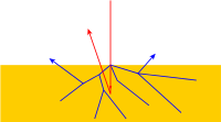
In addition to producing secondary electrons, primary electrons from the incident beam with sufficient energy to penetrate the resist can be multiply scattered over large distances from underlying films and/or the substrate. This leads to exposure of areas at a significant distance from the desired exposure location. For thicker resists, as the primary electrons move forward, they have an increasing opportunity to scatter laterally from the beam-defined location. This scattering is called forward scattering. Sometimes the primary electrons are scattered at angles exceeding 90 degrees, i.e., they no longer advance further into the resist. These electrons are called backscattered electrons and have the same effect as long-range flare in optical projection systems. A large enough dose of backscattered electrons can lead to complete exposure of resist over an area much larger than defined by the beam spot.
Proximity effect edit
The smallest features produced by electron-beam lithography have generally been isolated features, as nested features exacerbate the proximity effect, whereby electrons from exposure of an adjacent region spill over into the exposure of the currently written feature, effectively enlarging its image, and reducing its contrast, i.e., difference between maximum and minimum intensity. Hence, nested feature resolution is harder to control. For most resists, it is difficult to go below 25 nm lines and spaces, and a limit of 20 nm lines and spaces has been found.[26] In actuality, though, the range of secondary electron scattering is quite far, sometimes exceeding 100 nm,[27] but becoming very significant below 30 nm.[28]
The proximity effect is also manifest by secondary electrons leaving the top surface of the resist and then returning some tens of nanometers distance away.[29]
Proximity effects (due to electron scattering) can be addressed by solving the inverse problem and calculating the exposure function E(x,y) that leads to a dose distribution as close as possible to the desired dose D(x,y) when convolved by the scattering distribution point spread function PSF(x,y). However, it must be remembered that an error in the applied dose (e.g., from shot noise) would cause the proximity effect correction to fail.
Charging edit
Since electrons are charged particles, they tend to charge the substrate negatively unless they can quickly gain access to a path to ground. For a high-energy beam incident on a silicon wafer, virtually all the electrons stop in the wafer where they can follow a path to ground. However, for a quartz substrate such as a photomask, the embedded electrons will take a much longer time to move to ground. Often the negative charge acquired by a substrate can be compensated or even exceeded by a positive charge on the surface due to secondary electron emission into the vacuum. The presence of a thin conducting layer above or below the resist is generally of limited use for high energy (50 keV or more) electron beams, since most electrons pass through the layer into the substrate. The charge dissipation layer is generally useful only around or below 10 keV, since the resist is thinner and most of the electrons either stop in the resist or close to the conducting layer. However, they are of limited use due to their high sheet resistance, which can lead to ineffective grounding.
The range of low-energy secondary electrons (the largest component of the free electron population in the resist-substrate system) which can contribute to charging is not a fixed number but can vary from 0 to as high as 50 nm (see section New frontiers and extreme ultraviolet lithography). Hence, resist-substrate charging is not repeatable and is difficult to compensate consistently. Negative charging deflects the electron beam away from the charged area while positive charging deflects the electron beam toward the charged area.
Electron-beam resist performance edit
Due to the scission efficiency generally being an order of magnitude higher than the crosslinking efficiency, most polymers used for positive-tone electron-beam lithography will also crosslink (and therefore become negative tone) at doses an order of magnitude higher than the doses used to cause scission in the polymer for positive tone exposure. In the case of PMMA, exposure of electrons at up to more than 1000 μC/cm2, the gradation curve corresponds to the curve of a “normal” positive process. Above 2000 μC/cm2, the recombinant crosslinking process prevails, and at about 7000 μC/cm2 the layer is completely crosslinked which makes the layer more insoluble than the unexposed initial layer. If negative PMMA structures should be used, a stronger developer than for the positive process is required.[30] Such large dose increases may be required to avoid shot noise effects.[31][32][33]
A study performed at the Naval Research Laboratory[34] indicated that low-energy (10–50 eV) electrons were able to damage ~30 nm thick PMMA films. The damage was manifest as a loss of material.
- For the popular electron-beam resist ZEP-520, a pitch resolution limit of 60 nm (30 nm lines and spaces), independent of thickness and beam energy, was found.[35]
- A 20 nm resolution had also been demonstrated using a 3 nm 100 keV electron beam and PMMA resist.[36] 20 nm unexposed gaps between exposed lines showed inadvertent exposure by secondary electrons.
- Hydrogen silsesquioxane (HSQ) is a negative tone resist that is capable of forming isolated 2-nm-wide lines and 10 nm periodic dot arrays (10 nm pitch) in very thin layers.[37] HSQ itself is similar to porous, hydrogenated SiO2. It may be used to etch silicon but not silicon dioxide or other similar dielectrics.
In 2018, a thiol-ene resist was developed that features native reactive surface groups, which allows the direct functionalization of the resist surface with biomolecules.[38]
New frontiers edit
To get around the secondary electron generation, it will be imperative to use low-energy electrons as the primary radiation to expose resist. Ideally, these electrons should have energies on the order of not much more than several eV in order to expose the resist without generating any secondary electrons, since they will not have sufficient excess energy. Such exposure has been demonstrated using a scanning tunneling microscope as the electron beam source.[39] The data suggest that electrons with energies as low as 12 eV can penetrate 50 nm thick polymer resist. The drawback to using low energy electrons is that it is hard to prevent spreading of the electron beam in the resist.[40] Low energy electron optical systems are also hard to design for high resolution.[41] Coulomb inter-electron repulsion always becomes more severe for lower electron energy.

Another alternative in electron-beam lithography is to use extremely high electron energies (at least 100 keV) to essentially "drill" or sputter the material. This phenomenon has been observed frequently in transmission electron microscopy.[42] However, this is a very inefficient process, due to the inefficient transfer of momentum from the electron beam to the material. As a result, it is a slow process, requiring much longer exposure times than conventional electron beam lithography. Also high energy beams always bring up the concern of substrate damage.
Interference lithography using electron beams is another possible path for patterning arrays with nanometer-scale periods. A key advantage of using electrons over photons in interferometry is the much shorter wavelength for the same energy.
Despite the various intricacies and subtleties of electron beam lithography at different energies, it remains the most practical way to concentrate the most energy into the smallest area.
There has been significant interest in the development of multiple electron beam approaches to lithography in order to increase throughput. This work has been supported by SEMATECH and start-up companies such as Multibeam Corporation,[43] Mapper[44] and IMS.[45] IMS Nanofabrication has commercialized the multibeam-maskwriter and started a rollout in 2016.[46]
See also edit
References edit
- ^ McCord, M A.; Rooks, M.J. (2000). "2. Electron beam lithography". Microlithography. SPIE Handbook of Microlithography, Micromachining and Microfabrication. Vol. 1. Archived from the original on 2019-08-19. Retrieved 2007-01-04.
- ^ Parker, N. W.; et al. (2000). Dobisz, Elizabeth A. (ed.). "High-throughput NGL electron-beam direct-write lithography system". Proc. SPIE. Emerging Lithographic Technologies IV. 3997: 713. Bibcode:2000SPIE.3997..713P. doi:10.1117/12.390042. S2CID 109415718.
- ^ Faster and lower cost for 65 nm and 45 nm photomask patterning [dead link]
- ^ Kempsell, M.L.; Hendrickx, E.; Tritchkov, A.; Sakajiri, K.; Yasui, K.; Yoshitake, S.; Granik, Y.; Vandenberghe, G.; Smith, B.W. (2009). "Inverse lithography for 45-nm-node contact holes at 1.35 numerical aperture". Journal of Micro/Nanolithography, MEMS and MOEMS. 8 (4): 043001. doi:10.1117/1.3263702.
- ^ Sunaoshi, H.; Tachikawa, Y.; Higurashi, H.; Iijima, T.; Suzuki, J.; Kamikubo, T.; Ohtoshi, K.; Anze, H.; Katsumata, T.; Nakayamada, N.; Hara, S.; Tamamushi, S.; Ogawa, Y. (2006). "EBM-5000: electron-beam mask writer for 45-nm node". Photomask and Next-Generation Lithography Mask Technology XIII. SPIE Proceedings. Vol. 6283. p. 628306. doi:10.1117/12.681732.
- ^ Ugajin, K.; Saito, M.; Suenaga, M.; Higaki, T.; Nishino, H.; Watanabe, H.; Ikenaga, O. (2007). "1-nm of local CD accuracy for 45-nm-node photomask with low sensitivity CAR for e-beam writer". Photomask and Next-Generation Lithography Mask Technology XIV. SPIE Proceedings. Vol. 6607. pp. 90–97.
- ^ Chen, Frederick; Chen, Wei-Su; Tsai, Ming-Jinn; Ku, Tzu-Kun (2013). "Sidewall profile inclination modulation mask (SPIMM): modification of an attenuated phase-shift mask for single-exposure double and multiple patterning". Optical Microlithography XXVI. SPIE Proceedings. Vol. 8683. p. 868311. doi:10.1117/12.2008886.
- ^ The Significance of Point Spread Functions with Stochastic Behavior in Electron-Beam Lithography
- ^ Ichimura, Koji; Yoshida, Koji; Cho, Hideki; Hikichi, Ryugo; Kurihara, Masaaki (2022). "Characteristics of fine feature hole templates for nanoimprint lithography toward 2nm and beyond". Photomask Technology. SPIE Proceedings. Vol. 12293. pp. 122930F. doi:10.1117/12.2643250.
- ^ L. Feldman; J. Mayer (1986). Fundamentals of Surface and Thin Film Analysis. Vol. 54. North-Holland. pp. 130–133. ISBN 978-0-444-00989-0.
- ^ Mason, Nigel J; Dujardin, G; Gerber, G; Gianturco, F; Maerk, T.D. (January 2008). "EURONanochem – Chemical Control at the Nanoscale". Slovenian Research Agency. European Space Foundation. Archived from the original on 2011-07-20.
- ^ Stoffels, E; Stoffels, W W; Kroesen, G M W (2001). "Plasma chemistry and surface processes of negative ions". Plasma Sources Science and Technology. 10 (2): 311. Bibcode:2001PSST...10..311S. CiteSeerX 10.1.1.195.9811. doi:10.1088/0963-0252/10/2/321. S2CID 250916447.
- ^ Seah, M. P.; Dench, W. A. (1979). "Quantitative electron spectroscopy of surfaces: A standard data base for electron inelastic mean free paths in solids". Surface and Interface Analysis. 1: 2. doi:10.1002/sia.740010103.
- ^ Tanuma, S.; Powell, C. J.; Penn, D. R. (1994). "Calculations of electron inelastic mean free paths. V. Data for 14 organic compounds over the 50–2000 eV range". Surface and Interface Analysis. 21 (3): 165. doi:10.1002/sia.740210302.
- ^ a b Broers, A. N.; et al. (1996). "Electron beam lithography—Resolution limits". Microelectronic Engineering. 32 (1–4): 131–142. doi:10.1016/0167-9317(95)00368-1.
- ^ K. W. Lee (2009). "Secondary electron generation in electron-beam-irradiated solids:resolution limits to nanolithography". J. Korean Phys. Soc. 55 (4): 1720. Bibcode:2009JKPS...55.1720L. doi:10.3938/jkps.55.1720. Archived from the original on 2011-07-22.
- ^ SPIE Newsroom: Double exposure makes dense high-resolution diffractive optics. Spie.org (2009-11-03). Retrieved on 2011-08-27.
- ^ Dapor, M.; et al. (2010). "Monte Carlo modeling in the low-energy domain of the secondary electron emission of polymethylmethacrylate for critical-dimension scanning electron microscopy". J. Micro/Nanolith. MEMS MOEMS. 9 (2): 023001. doi:10.1117/1.3373517.
- ^ P. T. Henderson; et al. (1999). "Long-distance charge transport in duplex DNA: The phonon-assisted polaron-like hopping mechanism". Proc. Natl. Acad. Sci. U.S.A. 96 (15): 8353–8358. Bibcode:1999PNAS...96.8353H. doi:10.1073/pnas.96.15.8353. PMC 17521. PMID 10411879.
- ^ H. Seiler (1983). "Secondary electron emission in the scanning electron microscope". J. Appl. Phys. 54 (11): R1–R18. Bibcode:1983JAP....54R...1S. doi:10.1063/1.332840.
- ^ Denbeaux, G.; Torok, J.; Del Re, R.; Herbol, H.; Das, S.; Bocharova, I.; Paolucci, A.; Ocola, L.E.; Ventrice Jr., C.; Lifshin, E.; Brainard, R.L. (2013). "Measurement of the role of secondary electrons in EUV resist exposures" (PDF). International Workshop on EUV Lithography.
- ^ Complexities of the Resolution Limits of Advanced Lithography
- ^ Resolution Limits
- ^ Chen, Frederick (2023). Electron Blur Impact on Electron Beam and EUV Lithography.
- ^ Chandramouli, M.; Liu, B.; Alberti, Z.; Abboud, F.; Hochleitner, G.; Wroczewski, W.; Kuhn, S.; Klein, C.; Platzgummer, E. (2022). "Multibeam mask requirements for advanced EUV patterning". Photomask Technology. SPIE Proceedings. Vol. 12293. pp. 122930O. doi:10.1117/12.2645895.
- ^ J. A. Liddle; et al. (2003). "Resist Requirements and Limitations for Nanoscale Electron-Beam Patterning". Mater. Res. Soc. Symp. Proc. 739 (19): 19–30.[permanent dead link]
- ^ Ivin, V (2002). "The inclusion of secondary electrons and Bremsstrahlung X-rays in an electron beam resist model". Microelectronic Engineering. 61–62: 343. doi:10.1016/S0167-9317(02)00531-2.
- ^ Yamazaki, Kenji; Kurihara, Kenji; Yamaguchi, Toru; Namatsu, Hideo; Nagase, Masao (1997). "Novel Proximity Effect Including Pattern-Dependent Resist Development in Electron Beam Nanolithography". Japanese Journal of Applied Physics. 36 (12B): 7552. Bibcode:1997JaJAP..36.7552Y. doi:10.1143/JJAP.36.7552. S2CID 250783039.
- ^ Renoud, R; Attard, C; Ganachaud, J-P; Bartholome, S; Dubus, A (1998). "Influence on the secondary electron yield of the space charge induced in an insulating target by an electron beam". Journal of Physics: Condensed Matter. 10 (26): 5821. Bibcode:1998JPCM...10.5821R. doi:10.1088/0953-8984/10/26/010. S2CID 250739239.
- ^ J. N. Helbert et al., Macromolecules, vol. 11, 1104 (1978).
- ^ Wieland, M.; de Boer, G.; ten Berge, G.; Jager, R.; van de Peut, T.; Peijster, J.; Slot, E.; Steenbrink, S.; Teepen, T.; van Veen, A.H.V.; Kampherbeek, B.J. (2009). "MAPPER: high-throughput maskless lithography". Alternative Lithographic Technologies. SPIE Proceedings. Vol. 7271. pp. 72710O. doi:10.1117/12.814025.
- ^ Chen, Frederick; Chen, Wei-Su; Tsai, Ming-Jinn; Ku, Tzu-Kun (2012). "Complementary polarity exposures for cost-effective line-cutting in multiple patterning lithography". Optical Microlithography XXV. SPIE Proceedings. Vol. 8326. pp. 83262L. doi:10.1117/12.912800.
- ^ Kruit, P.; Steenbrink, S.; Jager, R.; Wieland, M. (2004). "Optimum dose for shot noise limited CD uniformity in electron-beam lithography". J. Vac. Sci. Tech. B. 22 (6): 2948–55. doi:10.1116/1.1821577.
- ^ Bermudez, V. M. (1999). "Low-energy electron-beam effects on poly(methyl methacrylate) resist films". Journal of Vacuum Science and Technology B. 17 (6): 2512. Bibcode:1999JVSTB..17.2512B. doi:10.1116/1.591134.
- ^ H. Yang et al., Proceedings of the 1st IEEE Intl. Conf. on Nano/Micro Engineered and Molecular Systems, pp. 391–394 (2006).
- ^ Cumming, D. R. S.; Thoms, S.; Beaumont, S. P.; Weaver, J. M. R. (1996). "Fabrication of 3 nm wires using 100 keV electron beam lithography and poly(methyl methacrylate) resist". Applied Physics Letters. 68 (3): 322. Bibcode:1996ApPhL..68..322C. doi:10.1063/1.116073.
- ^ Manfrinato, Vitor R.; Zhang, Lihua; Su, Dong; Duan, Huigao; Hobbs, Richard G.; Stach, Eric A.; Berggren, Karl K. (2013). "Resolution limits of electron-beam lithography toward the atomic scale" (PDF). Nano Lett. 13 (4): 1555–1558. Bibcode:2013NanoL..13.1555M. doi:10.1021/nl304715p. hdl:1721.1/92829. PMID 23488936. S2CID 1060983.
- ^ Shafagh, Reza; Vastesson, Alexander; Guo, Weijin; van der Wijngaart, Wouter; Haraldsson, Tommy (2018). "E-Beam Nanostructuring and Direct Click Biofunctionalization of Thiol–Ene Resist". ACS Nano. 12 (10): 9940–6. doi:10.1021/acsnano.8b03709. PMID 30212184. S2CID 52271550.
- ^ Marrian, C.R.K. (1992). "Electron-beam lithography with the scanning tunneling microscope". Journal of Vacuum Science and Technology. 10 (B): 2877–81. Bibcode:1992JVSTB..10.2877M. doi:10.1116/1.585978.
- ^ Mayer, T.M.; et al. (1996). "Field emission characteristics of the scanning tunneling microscope for nanolithography". Journal of Vacuum Science and Technology. 14 (B): 2438–44. Bibcode:1996JVSTB..14.2438M. doi:10.1116/1.588751.
- ^ Hordon, L.S.; et al. (1993). "Limits of low-energy electron optics". Journal of Vacuum Science and Technology. 11 (B): 2299–2303. Bibcode:1993JVSTB..11.2299H. doi:10.1116/1.586894.
- ^ Egerton, R. F.; et al. (2004). "Radiation damage in the TEM and SEM". Micron. 35 (6): 399–409. doi:10.1016/j.micron.2004.02.003. PMID 15120123.
- ^ Multibeam Corporation. Multibeamcorp.com (2011-03-04). Retrieved on 2011-08-27.
- ^ Mapper Lithography Archived 2016-12-20 at the Wayback Machine. Mapper Lithography (2010-01-18). Retrieved on 2011-08-27.
- ^ IMS Nanofabrications. IMS Nanofabrication(2011-12-07). Retrieved on 2019-02-28.
- ^ IMS Nanofabrications. IMS Nanofabrication(2011-12-07). Retrieved on 2019-02-28.