


Summary
In solid-state physics, the electronic band structure (or simply band structure) of a solid describes the range of energy levels that electrons may have within it, as well as the ranges of energy that they may not have (called band gaps or forbidden bands).
Band theory derives these bands and band gaps by examining the allowed quantum mechanical wave functions for an electron in a large, periodic lattice of atoms or molecules. Band theory has been successfully used to explain many physical properties of solids, such as electrical resistivity and optical absorption, and forms the foundation of the understanding of all solid-state devices (transistors, solar cells, etc.).
Why bands and band gaps occur edit
The formation of electronic bands and band gaps can be illustrated with two complementary models for electrons in solids.[1]: 161 The first one is the nearly free electron model, in which the electrons are assumed to move almost freely within the material. In this model, the electronic states resemble free electron plane waves, and are only slightly perturbed by the crystal lattice. This model explains the origin of the electronic dispersion relation, but the explanation for the band gaps is subtle in this model.[2]: 121
The second model starts from the opposite limit, in which the electrons are tightly bound to individual atoms. The electrons of a single, isolated atom occupy atomic orbitals with discrete energy levels. If two atoms come close enough so that their atomic orbitals overlap, the electrons can tunnel between the atoms. This tunneling splits (hybridizes) the atomic orbitals into molecular orbitals with different energies.[2]: 117–122
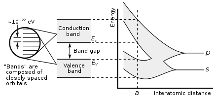
Similarly, if a large number N of identical atoms come together to form a solid, such as a crystal lattice, the atoms' atomic orbitals overlap with the nearby orbitals.[3] Each discrete energy level splits into N levels, each with a different energy. Since the number of atoms in a macroscopic piece of solid is a very large number (N~1022) the number of orbitals is very large and thus they are very closely spaced in energy (of the order of 10−22 eV). The energy of the adjacent levels is so close together that they can be considered as a continuum, an energy band.
This formation of bands is mostly a feature of the outermost electrons (valence electrons) in the atom, which are the ones involved in chemical bonding and electrical conductivity. The inner electron orbitals do not overlap to a significant degree, so their bands are very narrow.
Band gaps are essentially leftover ranges of energy not covered by any band, a result of the finite widths of the energy bands. The bands have different widths, with the widths depending upon the degree of overlap in the atomic orbitals from which they arise. Two adjacent bands may simply not be wide enough to fully cover the range of energy. For example, the bands associated with core orbitals (such as 1s electrons) are extremely narrow due to the small overlap between adjacent atoms. As a result, there tend to be large band gaps between the core bands. Higher bands involve comparatively larger orbitals with more overlap, becoming progressively wider at higher energies so that there are no band gaps at higher energies.
Basic concepts edit
Assumptions and limits of band structure theory edit
Band theory is only an approximation to the quantum state of a solid, which applies to solids consisting of many identical atoms or molecules bonded together. These are the assumptions necessary for band theory to be valid:
- Infinite-size system: For the bands to be continuous, the piece of material must consist of a large number of atoms. Since a macroscopic piece of material contains on the order of 1022 atoms, this is not a serious restriction; band theory even applies to microscopic-sized transistors in integrated circuits. With modifications, the concept of band structure can also be extended to systems which are only "large" along some dimensions, such as two-dimensional electron systems.
- Homogeneous system: Band structure is an intrinsic property of a material, which assumes that the material is homogeneous. Practically, this means that the chemical makeup of the material must be uniform throughout the piece.
- Non-interactivity: The band structure describes "single electron states". The existence of these states assumes that the electrons travel in a static potential without dynamically interacting with lattice vibrations, other electrons, photons, etc.
The above assumptions are broken in a number of important practical situations, and the use of band structure requires one to keep a close check on the limitations of band theory:
- Inhomogeneities and interfaces: Near surfaces, junctions, and other inhomogeneities, the bulk band structure is disrupted. Not only are there local small-scale disruptions (e.g., surface states or dopant states inside the band gap), but also local charge imbalances. These charge imbalances have electrostatic effects that extend deeply into semiconductors, insulators, and the vacuum (see doping, band bending).
- Along the same lines, most electronic effects (capacitance, electrical conductance, electric-field screening) involve the physics of electrons passing through surfaces and/or near interfaces. The full description of these effects, in a band structure picture, requires at least a rudimentary model of electron-electron interactions (see space charge, band bending).
- Small systems: For systems which are small along every dimension (e.g., a small molecule or a quantum dot), there is no continuous band structure. The crossover between small and large dimensions is the realm of mesoscopic physics.
- Strongly correlated materials (for example, Mott insulators) simply cannot be understood in terms of single-electron states. The electronic band structures of these materials are poorly defined (or at least, not uniquely defined) and may not provide useful information about their physical state.
Crystalline symmetry and wavevectors edit


Band structure calculations take advantage of the periodic nature of a crystal lattice, exploiting its symmetry. The single-electron Schrödinger equation is solved for an electron in a lattice-periodic potential, giving Bloch electrons as solutions

The wavevector takes on any value inside the Brillouin zone, which is a polyhedron in wavevector (reciprocal lattice) space that is related to the crystal's lattice. Wavevectors outside the Brillouin zone simply correspond to states that are physically identical to those states within the Brillouin zone. Special high symmetry points/lines in the Brillouin zone are assigned labels like Γ, Δ, Λ, Σ (see Fig 1).
It is difficult to visualize the shape of a band as a function of wavevector, as it would require a plot in four-dimensional space, E vs. kx, ky, kz. In scientific literature it is common to see band structure plots which show the values of En(k) for values of k along straight lines connecting symmetry points, often labelled Δ, Λ, Σ, or [100], [111], and [110], respectively.[4][5] Another method for visualizing band structure is to plot a constant-energy isosurface in wavevector space, showing all of the states with energy equal to a particular value. The isosurface of states with energy equal to the Fermi level is known as the Fermi surface.
Energy band gaps can be classified using the wavevectors of the states surrounding the band gap:
- Direct band gap: the lowest-energy state above the band gap has the same k as the highest-energy state beneath the band gap.
- Indirect band gap: the closest states above and beneath the band gap do not have the same k value.
Asymmetry: Band structures in non-crystalline solids edit
Although electronic band structures are usually associated with crystalline materials, quasi-crystalline and amorphous solids may also exhibit band gaps. These are somewhat more difficult to study theoretically since they lack the simple symmetry of a crystal, and it is not usually possible to determine a precise dispersion relation. As a result, virtually all of the existing theoretical work on the electronic band structure of solids has focused on crystalline materials.
Density of states edit
The density of states function g(E) is defined as the number of electronic states per unit volume, per unit energy, for electron energies near E.
The density of states function is important for calculations of effects based on band theory. In Fermi's Golden Rule, a calculation for the rate of optical absorption, it provides both the number of excitable electrons and the number of final states for an electron. It appears in calculations of electrical conductivity where it provides the number of mobile states, and in computing electron scattering rates where it provides the number of final states after scattering.[citation needed]
For energies inside a band gap, g(E) = 0.
Filling of bands edit

At thermodynamic equilibrium, the likelihood of a state of energy E being filled with an electron is given by the Fermi–Dirac distribution, a thermodynamic distribution that takes into account the Pauli exclusion principle:

- kBT is the product of Boltzmann's constant and temperature, and
- µ is the total chemical potential of electrons, or Fermi level (in semiconductor physics, this quantity is more often denoted EF). The Fermi level of a solid is directly related to the voltage on that solid, as measured with a voltmeter. Conventionally, in band structure plots the Fermi level is taken to be the zero of energy (an arbitrary choice).
The density of electrons in the material is simply the integral of the Fermi–Dirac distribution times the density of states:

Although there are an infinite number of bands and thus an infinite number of states, there are only a finite number of electrons to place in these bands. The preferred value for the number of electrons is a consequence of electrostatics: even though the surface of a material can be charged, the internal bulk of a material prefers to be charge neutral. The condition of charge neutrality means that N/V must match the density of protons in the material. For this to occur, the material electrostatically adjusts itself, shifting its band structure up or down in energy (thereby shifting g(E)), until it is at the correct equilibrium with respect to the Fermi level.
Names of bands near the Fermi level (conduction band, valence band) edit
A solid has an infinite number of allowed bands, just as an atom has infinitely many energy levels. However, most of the bands simply have too high energy, and are usually disregarded under ordinary circumstances.[6] Conversely, there are very low energy bands associated with the core orbitals (such as 1s electrons). These low-energy core bands are also usually disregarded since they remain filled with electrons at all times, and are therefore inert.[7] Likewise, materials have several band gaps throughout their band structure.
The most important bands and band gaps—those relevant for electronics and optoelectronics—are those with energies near the Fermi level. The bands and band gaps near the Fermi level are given special names, depending on the material:
- In a semiconductor or band insulator, the Fermi level is surrounded by a band gap, referred to as the band gap (to distinguish it from the other band gaps in the band structure). The closest band above the band gap is called the conduction band, and the closest band beneath the band gap is called the valence band. The name "valence band" was coined by analogy to chemistry, since in semiconductors (and insulators) the valence band is built out of the valence orbitals.
- In a metal or semimetal, the Fermi level is inside of one or more allowed bands. In semimetals the bands are usually referred to as "conduction band" or "valence band" depending on whether the charge transport is more electron-like or hole-like, by analogy to semiconductors. In many metals, however, the bands are neither electron-like nor hole-like, and often just called "valence band" as they are made of valence orbitals.[8] The band gaps in a metal's band structure are not important for low energy physics, since they are too far from the Fermi level.
Theory in crystals edit
The ansatz is the special case of electron waves in a periodic crystal lattice using Bloch's theorem as treated generally in the dynamical theory of diffraction. Every crystal is a periodic structure which can be characterized by a Bravais lattice, and for each Bravais lattice we can determine the reciprocal lattice, which encapsulates the periodicity in a set of three reciprocal lattice vectors (b1, b2, b3). Now, any periodic potential V(r) which shares the same periodicity as the direct lattice can be expanded out as a Fourier series whose only non-vanishing components are those associated with the reciprocal lattice vectors. So the expansion can be written as:

From this theory, an attempt can be made to predict the band structure of a particular material, however most ab initio methods for electronic structure calculations fail to predict the observed band gap.
Nearly free electron approximation edit
In the nearly free electron approximation, interactions between electrons are completely ignored. This approximation allows use of Bloch's Theorem which states that electrons in a periodic potential have wavefunctions and energies which are periodic in wavevector up to a constant phase shift between neighboring reciprocal lattice vectors. The consequences of periodicity are described mathematically by the Bloch's theorem, which states that the eigenstate wavefunctions have the form


Here index n refers to the n-th energy band, wavevector k is related to the direction of motion of the electron, r is the position in the crystal, and R is the location of an atomic site.[9]: 179
The NFE model works particularly well in materials like metals where distances between neighbouring atoms are small. In such materials the overlap of atomic orbitals and potentials on neighbouring atoms is relatively large. In that case the wave function of the electron can be approximated by a (modified) plane wave. The band structure of a metal like aluminium even gets close to the empty lattice approximation.
Tight binding model edit
The opposite extreme to the nearly free electron approximation assumes the electrons in the crystal behave much like an assembly of constituent atoms. This tight binding model assumes the solution to the time-independent single electron Schrödinger equation is well approximated by a linear combination of atomic orbitals .[9]: 245–248


The TB model works well in materials with limited overlap between atomic orbitals and potentials on neighbouring atoms. Band structures of materials like Si, GaAs, SiO2 and diamond for instance are well described by TB-Hamiltonians on the basis of atomic sp3 orbitals. In transition metals a mixed TB-NFE model is used to describe the broad NFE conduction band and the narrow embedded TB d-bands. The radial functions of the atomic orbital part of the Wannier functions are most easily calculated by the use of pseudopotential methods. NFE, TB or combined NFE-TB band structure calculations,[11] sometimes extended with wave function approximations based on pseudopotential methods, are often used as an economic starting point for further calculations.
KKR model edit
The KKR method, also called "multiple scattering theory" or Green's function method, finds the stationary values of the inverse transition matrix T rather than the Hamiltonian. A variational implementation was suggested by Korringa, Kohn and Rostocker, and is often referred to as the Korringa–Kohn–Rostoker method.[12][13] The most important features of the KKR or Green's function formulation are (1) it separates the two aspects of the problem: structure (positions of the atoms) from the scattering (chemical identity of the atoms); and (2) Green's functions provide a natural approach to a localized description of electronic properties that can be adapted to alloys and other disordered system. The simplest form of this approximation centers non-overlapping spheres (referred to as muffin tins) on the atomic positions. Within these regions, the potential experienced by an electron is approximated to be spherically symmetric about the given nucleus. In the remaining interstitial region, the screened potential is approximated as a constant. Continuity of the potential between the atom-centered spheres and interstitial region is enforced.
Density-functional theory edit
In recent physics literature, a large majority of the electronic structures and band plots are calculated using density-functional theory (DFT), which is not a model but rather a theory, i.e., a microscopic first-principles theory of condensed matter physics that tries to cope with the electron-electron many-body problem via the introduction of an exchange-correlation term in the functional of the electronic density. DFT-calculated bands are in many cases found to be in agreement with experimentally measured bands, for example by angle-resolved photoemission spectroscopy (ARPES). In particular, the band shape is typically well reproduced by DFT. But there are also systematic errors in DFT bands when compared to experiment results. In particular, DFT seems to systematically underestimate by about 30-40% the band gap in insulators and semiconductors.[14]
It is commonly believed that DFT is a theory to predict ground state properties of a system only (e.g. the total energy, the atomic structure, etc.), and that excited state properties cannot be determined by DFT. This is a misconception. In principle, DFT can determine any property (ground state or excited state) of a system given a functional that maps the ground state density to that property. This is the essence of the Hohenberg–Kohn theorem.[15] In practice, however, no known functional exists that maps the ground state density to excitation energies of electrons within a material. Thus, what in the literature is quoted as a DFT band plot is a representation of the DFT Kohn–Sham energies, i.e., the energies of a fictive non-interacting system, the Kohn–Sham system, which has no physical interpretation at all. The Kohn–Sham electronic structure must not be confused with the real, quasiparticle electronic structure of a system, and there is no Koopmans' theorem holding for Kohn–Sham energies, as there is for Hartree–Fock energies, which can be truly considered as an approximation for quasiparticle energies. Hence, in principle, Kohn–Sham based DFT is not a band theory, i.e., not a theory suitable for calculating bands and band-plots. In principle time-dependent DFT can be used to calculate the true band structure although in practice this is often difficult. A popular approach is the use of hybrid functionals, which incorporate a portion of Hartree–Fock exact exchange; this produces a substantial improvement in predicted bandgaps of semiconductors, but is less reliable for metals and wide-bandgap materials.[16]
Green's function methods and the ab initio GW approximation edit
To calculate the bands including electron-electron interaction many-body effects, one can resort to so-called Green's function methods. Indeed, knowledge of the Green's function of a system provides both ground (the total energy) and also excited state observables of the system. The poles of the Green's function are the quasiparticle energies, the bands of a solid. The Green's function can be calculated by solving the Dyson equation once the self-energy of the system is known. For real systems like solids, the self-energy is a very complex quantity and usually approximations are needed to solve the problem. One such approximation is the GW approximation, so called from the mathematical form the self-energy takes as the product Σ = GW of the Green's function G and the dynamically screened interaction W. This approach is more pertinent when addressing the calculation of band plots (and also quantities beyond, such as the spectral function) and can also be formulated in a completely ab initio way. The GW approximation seems to provide band gaps of insulators and semiconductors in agreement with experiment, and hence to correct the systematic DFT underestimation.
Dynamical mean-field theory edit
Although the nearly free electron approximation is able to describe many properties of electron band structures, one consequence of this theory is that it predicts the same number of electrons in each unit cell. If the number of electrons is odd, we would then expect that there is an unpaired electron in each unit cell, and thus that the valence band is not fully occupied, making the material a conductor. However, materials such as CoO that have an odd number of electrons per unit cell are insulators, in direct conflict with this result. This kind of material is known as a Mott insulator, and requires inclusion of detailed electron-electron interactions (treated only as an averaged effect on the crystal potential in band theory) to explain the discrepancy. The Hubbard model is an approximate theory that can include these interactions. It can be treated non-perturbatively within the so-called dynamical mean-field theory, which attempts to bridge the gap between the nearly free electron approximation and the atomic limit. Formally, however, the states are not non-interacting in this case and the concept of a band structure is not adequate to describe these cases.
Others edit
Calculating band structures is an important topic in theoretical solid state physics. In addition to the models mentioned above, other models include the following:
- Empty lattice approximation: the "band structure" of a region of free space that has been divided into a lattice.
- k·p perturbation theory is a technique that allows a band structure to be approximately described in terms of just a few parameters. The technique is commonly used for semiconductors, and the parameters in the model are often determined by experiment.
- The Kronig–Penney model, a one-dimensional rectangular well model useful for illustration of band formation. While simple, it predicts many important phenomena, but is not quantitative.
- Hubbard model
The band structure has been generalised to wavevectors that are complex numbers, resulting in what is called a complex band structure, which is of interest at surfaces and interfaces.
Each model describes some types of solids very well, and others poorly. The nearly free electron model works well for metals, but poorly for non-metals. The tight binding model is extremely accurate for ionic insulators, such as metal halide salts (e.g. NaCl).
Band diagrams edit
To understand how band structure changes relative to the Fermi level in real space, a band structure plot is often first simplified in the form of a band diagram. In a band diagram the vertical axis is energy while the horizontal axis represents real space. Horizontal lines represent energy levels, while blocks represent energy bands. When the horizontal lines in these diagram are slanted then the energy of the level or band changes with distance. Diagrammatically, this depicts the presence of an electric field within the crystal system. Band diagrams are useful in relating the general band structure properties of different materials to one another when placed in contact with each other.
See also edit
- Band-gap engineering—the process of altering a material's band structure
- Felix Bloch—pioneer in the theory of band structure
- Alan Herries Wilson—pioneer in the theory of band structure
References edit
- ^ Simon, Steven H. (2013). The Oxford Solid State Basics. Oxford: Oxford University Press. ISBN 978-0-19-150210-1.
- ^ a b Girvin, Steven M.; Yang, Kun (2019). Modern Condensed Matter Physics. Cambridge: Cambridge University Press. ISBN 978-1-107-13739-4.
- ^ Holgate, Sharon Ann (2009). Understanding Solid State Physics. CRC Press. pp. 177–178. ISBN 978-1-4200-1232-3.
- ^ "NSM Archive - Aluminium Gallium Arsenide (AlGaAs) - Band structure and carrier concentration". www.ioffe.ru.
- ^ "Electronic Band Structure" (PDF). www.springer.com. Springer. p. 24. Retrieved 10 November 2016.
- ^ High-energy bands are important for electron diffraction physics, where the electrons can be injected into a material at high energies, see Stern, R.; Perry, J.; Boudreaux, D. (1969). "Low-Energy Electron-Diffraction Dispersion Surfaces and Band Structure in Three-Dimensional Mixed Laue and Bragg Reflections". Reviews of Modern Physics. 41 (2): 275. Bibcode:1969RvMP...41..275S. doi:10.1103/RevModPhys.41.275..
- ^ Low-energy bands are however important in the Auger effect.
- ^ In copper, for example, the effective mass is a tensor and also changes sign depending on the wave vector, as can be seen in the De Haas–Van Alphen effect; see https://www.phys.ufl.edu/fermisurface/
- ^ a b c Charles Kittel (1996). Introduction to Solid State Physics (Seventh ed.). New York: Wiley. ISBN 978-0-471-11181-8.
- ^ Daniel Charles Mattis (1994). The Many-Body Problem: Encyclopaedia of Exactly Solved Models in One Dimension. World Scientific. p. 340. ISBN 978-981-02-1476-0.
- ^ Walter Ashley Harrison (1989). Electronic Structure and the Properties of Solids. Dover Publications. ISBN 978-0-486-66021-9.
- ^ Joginder Singh Galsin (2001). Impurity Scattering in Metal Alloys. Springer. Appendix C. ISBN 978-0-306-46574-1.
- ^ Kuon Inoue, Kazuo Ohtaka (2004). Photonic Crystals. Springer. p. 66. ISBN 978-3-540-20559-3.
- ^ Assadi, M. Hussein. N.; Hanaor, Dorian A. H. (2013-06-21). "Theoretical study on copper's energetics and magnetism in TiO2 polymorphs". Journal of Applied Physics. 113 (23): 233913–233913–5. arXiv:1304.1854. Bibcode:2013JAP...113w3913A. doi:10.1063/1.4811539. ISSN 0021-8979. S2CID 94599250.
- ^ Hohenberg, P; Kohn, W. (Nov 1964). "Inhomogeneous Electron Gas". Phys. Rev. 136 (3B): B864–B871. Bibcode:1964PhRv..136..864H. doi:10.1103/PhysRev.136.B864.
- ^ Paier, J.; Marsman, M.; Hummer, K.; Kresse, G.; Gerber, I. C.; Angyán, J. G. (2006). "Screened hybrid density functionals applied to solids". J Chem Phys. 124 (15): 154709. Bibcode:2006JChPh.124o4709P. doi:10.1063/1.2187006. PMID 16674253.
Further reading edit
- Ashcroft, Neil and N. David Mermin, Solid State Physics, ISBN 0-03-083993-9
- Harrison, Walter A., Elementary Electronic Structure, ISBN 981-238-708-0
- Harrison, Walter A.; W. A. Benjamin Pseudopotentials in the theory of metals, (New York) 1966
- Marder, Michael P., Condensed Matter Physics, ISBN 0-471-17779-2
- Martin, Richard, Electronic Structure: Basic Theory and Practical Methods, ISBN 0-521-78285-6
- Millman, Jacob; Arvin Gabriel, Microelectronics, ISBN 0-07-463736-3, Tata McGraw-Hill Edition.
- Nemoshkalenko, V. V., and N. V. Antonov, Computational Methods in Solid State Physics, ISBN 90-5699-094-2
- Omar, M. Ali, Elementary Solid State Physics: Principles and Applications, ISBN 0-201-60733-6
- Singh, Jasprit, Electronic and Optoelectronic Properties of Semiconductor Structures Chapters 2 and 3, ISBN 0-521-82379-X
- Vasileska, Dragica, Tutorial on Bandstructure Methods (2008)