


Summary
Electrostatic discharge (ESD) is a sudden and momentary flow of electric current between two differently-charged objects when brought close together or when the dielectric between them breaks down, often creating a visible spark associated with the static electricity between the objects.
ESD can create spectacular electric sparks (lightning, with the accompanying sound of thunder, is an example of a large-scale ESD event), but also less dramatic forms which may be neither seen nor heard, yet still be large enough to cause damage to sensitive electronic devices. Electric sparks require a field strength above approximately 4 × 10⁶ V/m in air, as notably occurs in lightning strikes. Other forms of ESD include corona discharge from sharp electrodes, brush discharge from blunt electrodes, etc.
ESD can cause harmful effects of importance in industry, including explosions in gas, fuel vapor and coal dust, as well as failure of solid state electronics components such as integrated circuits. These can suffer permanent damage when subjected to high voltages. Electronics manufacturers therefore establish electrostatic protective areas free of static, using measures to prevent charging, such as avoiding highly charging materials and measures to remove static such as grounding human workers, providing antistatic devices, and controlling humidity.
ESD simulators may be used to test electronic devices, for example with a human body model or a charged device model.
Causes edit
One of the causes of ESD events is static electricity. Static electricity is often generated through tribocharging, the separation of electric charges that occurs when two materials are brought into contact and then separated. Examples of tribocharging include walking on a rug, rubbing a plastic comb against dry hair, rubbing a balloon against a sweater, ascending from a fabric car seat, or removing some types of plastic packaging. In all these cases, the breaking of contact between two materials results in tribocharging, thus creating a difference of electrical potential that can lead to an ESD event.
Another cause of ESD damage is through electrostatic induction. This occurs when an electrically charged object is placed near a conductive object isolated from the ground. The presence of the charged object creates an electrostatic field that causes electrical charges on the surface of the other object to redistribute. Even though the net electrostatic charge of the object has not changed, it now has regions of excess positive and negative charges. An ESD event may occur when the object comes into contact with a conductive path. For example, charged regions on the surfaces of styrofoam cups or bags can induce potential on nearby ESD sensitive components via electrostatic induction and an ESD event may occur if the component is touched with a metallic tool.
ESD can also be caused by energetic charged particles impinging on an object. This causes increasing surface and deep charging. This is a known hazard for most spacecraft.[1]
Types edit
Electrostatic discharge (ESD) phenomena vary in complexity and magnitude, with the electric spark being the most visible and dramatic example. This occurs when a strong electric field ionizes the air, creating a conductive channel that can convey an electric current. People may experience this as a small jolt of discomfort, but ESD can inflict severe damage on electronic components, potentially leading to malfunctions and failures. In hazardous environments where flammable gases or dust particles are present, ESD can trigger fires or explosions.
Not all ESD events, however, are accompanied by a visible spark or noise. It is possible for a person to carry a charge that, while undetectable to the human senses, can still be potent enough to harm delicate electronics. Some components can be compromised by discharges as faint as 30 V, with such damage sometimes not becoming apparent until significant usage has occurred, thus affecting the lifespan and performance of the devices.[citation needed]
Cable discharge events (CDEs) are discharges occurring when connecting electrical cables to a device.
Sparks edit
A spark is triggered when the electric field strength exceeds approximately 4–30 kV/cm[2] — the dielectric field strength of air. This may cause a very rapid increase in the number of free electrons and ions in the air, temporarily causing the air to abruptly become an electrical conductor in a process called dielectric breakdown.
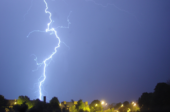
Perhaps the best known example of a natural spark is lightning. In this case the electric potential between a cloud and ground, or between two clouds, is typically hundreds of millions of volts. The resulting current that cycles through the stroke channel causes an enormous transfer of energy. On a much smaller scale, sparks can form in air during electrostatic discharges from charged objects that are charged to as little as 380 V (Paschen's law).
Earth's atmosphere consists of 21% oxygen (O2) and 78% nitrogen (N2). During an electrostatic discharge, such as a lightning flash, the affected atmospheric molecules become electrically overstressed. The diatomic oxygen molecules are split, and then recombine to form ozone (O3), which is unstable, or reacts with metals and organic matter. If the electrical stress is high enough, nitrogen oxides (NOx) can form. Both products are toxic to animals, and nitrogen oxides are essential for nitrogen fixation. Ozone attacks all organic matter by ozonolysis and is used in water purification.
Sparks are an ignition source in combustible environments that may lead to catastrophic explosions in concentrated fuel environments. Most explosions can be traced back to a tiny electrostatic discharge, whether it was an unexpected combustible fuel leak invading a known open air sparking device, or an unexpected spark in a known fuel rich environment. The result is the same if oxygen is present and the three criteria of the fire triangle have been combined.
Damage prevention in electronics edit

Many electronic components, especially integrated circuits and microchips, can be damaged by ESD. Sensitive components need to be protected during and after manufacture, during shipping and device assembly, and in the finished device. Grounding is especially important for effective ESD control. It should be clearly defined, and regularly evaluated.[3]
Protection during manufacturing edit

In manufacturing, prevention of ESD is based on an Electrostatic Discharge Protected Area (EPA). The EPA can be a small workstation or a large manufacturing area. The main principle of an EPA is that there are no highly-charging materials in the vicinity of ESD sensitive electronics, all conductive and dissipative materials are grounded, workers are grounded, and charge build-up on ESD sensitive electronics is prevented. International standards are used to define a typical EPA and can be found for example from International Electrotechnical Commission (IEC) or American National Standards Institute (ANSI).
ESD prevention within an EPA may include using appropriate ESD-safe packing material, the use of conductive filaments on garments worn by assembly workers, conducting wrist straps and foot-straps to prevent high voltages from accumulating on workers' bodies, anti-static mats or conductive flooring materials to conduct harmful electric charges away from the work area, and humidity control. Humid conditions prevent electrostatic charge generation because the thin layer of moisture that accumulates on most surfaces serves to dissipate electric charges.
Ionizers are used especially when insulative materials cannot be grounded. Ionization systems help to neutralize charged surface regions on insulative or dielectric materials. Insulating materials prone to triboelectric charging of more than 2,000 V should be kept away at least 12 inches from sensitive devices to prevent accidental charging of devices through field induction. On aircraft, static dischargers are used on the trailing edges of wings and other surfaces.
Manufacturers and users of integrated circuits must take precautions to avoid ESD. ESD prevention can be part of the device itself and include special design techniques for device input and output pins. External protection components can also be used with circuit layout.
Due to dielectric nature of electronics component and assemblies, electrostatic charging cannot be completely prevented during handling of devices. Most of ESD sensitive electronic assemblies and components are also so small that manufacturing and handling is done with automated equipment. ESD prevention activities are therefore important with those processes where components come into direct contact with equipment surfaces. In addition, it is important to prevent ESD when an electrostatic discharge sensitive component is connected with other conductive parts of the product itself. An efficient way to prevent ESD is to use materials that are not too conductive but will slowly conduct static charges away. These materials are called static dissipative and have resistivity values below 1012 ohm-meters. Materials in automated manufacturing which will touch on conductive areas of ESD sensitive electronic should be made of dissipative material, and the dissipative material must be grounded. These special materials are able to conduct electricity, but do so very slowly. Any built-up static charges dissipate without the sudden discharge that can harm the internal structure of silicon circuits.
Protection during transit edit
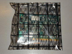
Sensitive devices need to be protected during shipping, handling, and storage. The buildup and discharge of static can be minimized by controlling the surface resistance and volume resistivity of packaging materials. Packaging is also designed to minimize frictional or triboelectric charging of packs due to rubbing together during shipping, and it may be necessary to incorporate electrostatic or electromagnetic shielding in the packaging material.[4] A common example is that semiconductor devices and computer components are usually shipped in an antistatic bag made of a partially conductive plastic, which acts as a Faraday cage to protect the contents against ESD.
Simulation and testing for electronic devices edit

For testing the susceptibility of electronic devices to ESD from human contact, an ESD Simulator with a special output circuit, called the human body model (HBM) is often used. This consists of a capacitor in series with a resistor. The capacitor is charged to a specified high voltage from an external source, and then suddenly discharged through the resistor into an electrical terminal of the device under test. One of the most widely used models is defined in the JEDEC 22-A114-B standard, which specifies a 100 picofarad capacitor and a 1,500 ohm resistor. Other similar standards are MIL-STD-883 Method 3015, and the ESD Association's ESD STM5.1. For compliance to European Union standards for Information Technology Equipment, the IEC/EN 61000-4-2 test specification is used.[5] Another specification referenced by equipment maker Schaffner calls for C = 150 pF and R = 330 Ω which provides high fidelity results. While the theory is mostly there, very few companies measure the real ESD survival rate. Guidelines and requirements are given for test cell geometries, generator specifications, test levels, discharge rate and waveform, types and points of discharge on the "victim" product, and functional criteria for gauging product survivability.
A charged device model (CDM) test is used to define the ESD a device can withstand when the device itself has an electrostatic charge and discharges due to metal contact. This discharge type is the most common type of ESD in electronic devices and causes most of the ESD damages in their manufacturing. CDM discharge depends mainly on parasitic parameters of the discharge and strongly depends on size and type of component package. One of the most widely used CDM simulation test models is defined by the JEDEC.
Other standardized ESD test circuits include the machine model (MM) and transmission line pulse (TLP).
See also edit
- Automotive Electronics Council, which defines in some of its standards, ESD test qualification requirements for electronic components used in vehicles
- Dielectric wireless receiver
- Electric arc
- Electromagnetic pulse
- Electrostatic voltmeter
- ESD Association, the industry leader in electrostatic discharge education and standards.
- ESD turnstile
- ggNMOS
- Latchup, for qualification testing of semiconductor devices, ESD and latchup are commonly considered together
- Spark gap
- Static electricity
- Wimshurst machine
References edit
- ^ Henry B. Garrett and Albert C. Whittlesey: Spacecraft charging, an update; IEEE Trans. Plasma Science, 28(6), 2000.
- ^ CRC Handbook of Chemistry and Physics (PDF)
- ^ "Fundamentals of Electrostatic Discharge". In Compliance Magazine. May 1, 2015. Retrieved 25 June 2015.
- ^ GR-1421, Generic Requirements for ESD-Protective Circuit Packed Containers, Telcordia.
- ^ "Baytems ESDzap - Lightweight ESD Simulator Product Overview" (PDF). Baytems. Aug 25, 2012. Retrieved 2012-08-25.
External links edit
- ESD Association
 Media related to Electrostatic discharge at Wikimedia Commons