


Summary
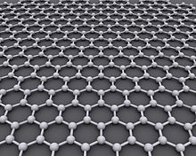
Graphene (/ˈɡræfiːn/[1]) is an allotrope of carbon consisting of a single layer of atoms arranged in a hexagonal lattice[2][3] nanostructure.[4] The name is derived from "graphite" and the suffix -ene, reflecting the fact that the graphite allotrope of carbon contains numerous double bonds.
Each atom in a graphene sheet is connected to its three nearest neighbors by σ-bonds and a delocalised π-bond, which contributes to a valence band that extends over the whole sheet. This is the same type of bonding seen in carbon nanotubes and polycyclic aromatic hydrocarbons, and (partially) in fullerenes and glassy carbon.[5][6] The valence band is touched by a conduction band, making graphene a semimetal with unusual electronic properties that are best described by theories for massless relativistic particles.[2] Charge carriers in graphene show linear, rather than quadratic, dependence of energy on momentum, and field-effect transistors with graphene can be made that show bipolar conduction. Charge transport is ballistic over long distances; the material exhibits large quantum oscillations and large and nonlinear diamagnetism.[7] Graphene conducts heat and electricity very efficiently along its plane. The material strongly absorbs light of all visible wavelengths,[8][9] which accounts for the black color of graphite, yet a single graphene sheet is nearly transparent because of its extreme thinness. Microscopically, graphene is the strongest material ever measured.[10][11]

Scientists theorized the potential existence and production of graphene for decades. It has likely been unknowingly produced in small quantities for centuries, through the use of pencils and other similar applications of graphite. It was possibly observed in electron microscopes in 1962, but studied only while supported on metal surfaces.[12]
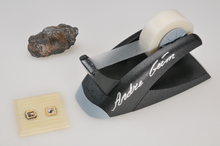
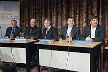
In 2004, the material was rediscovered, isolated and investigated at the University of Manchester,[13][14] by Andre Geim and Konstantin Novoselov. In 2010, Geim and Novoselov were awarded the Nobel Prize in Physics for their "groundbreaking experiments regarding the two-dimensional material graphene".[15] High-quality graphene proved to be surprisingly easy to isolate.
Graphene has become a valuable and useful nanomaterial due to its exceptionally high tensile strength, electrical conductivity, transparency, and being the thinnest two-dimensional material in the world.[4] The global market for graphene was $9 million in 2012,[16] with most of the demand from research and development in semiconductor, electronics, electric batteries,[17] and composites.
The IUPAC (International Union for Pure and Applied Chemistry) recommends use of the name "graphite" for the three-dimensional material, and "graphene" only when the reactions, structural relations, or other properties of individual layers are discussed.[18] A narrower definition, of "isolated or free-standing graphene" requires that the layer be sufficiently isolated from its environment,[19] but would include layers suspended or transferred to silicon dioxide or silicon carbide.[20]
History edit
Structure of graphite and its intercalation compounds edit
In 1859, Benjamin Brodie noted the highly lamellar structure of thermally reduced graphite oxide.[21][22] In 1916, Peter Debye and Paul Scherrer determined the structure of graphite by powder X-ray diffraction.[23][24][25] The structure was studied in more detail by V. Kohlschütter and P. Haenni in 1918, who also described the properties of graphite oxide paper.[26] Its structure was determined from single-crystal diffraction in 1924.[27][28]
The theory of graphene was first explored by P. R. Wallace in 1947 as a starting point for understanding the electronic properties of 3D graphite. The emergent massless Dirac equation was first pointed out in 1984 separately by Gordon Walter Semenoff,[29] and by David P. DiVincenzo and Eugene J. Mele.[30] Semenoff emphasized the occurrence in a magnetic field of an electronic Landau level precisely at the Dirac point. This level is responsible for the anomalous integer quantum Hall effect.[31][32][33]
edit
Transmission electron microscopy (TEM) images of thin graphite samples consisting of a few graphene layers were published by G. Ruess and F. Vogt in 1948.[34] Eventually, single layers were also observed directly.[35] Single layers of graphite were also observed by transmission electron microscopy within bulk materials, in particular inside soot obtained by chemical exfoliation.[6]
In 1961–1962, Hanns-Peter Boehm published a study of extremely thin flakes of graphite, and coined the term "graphene" for the hypothetical single-layer structure.[36] This paper reports graphitic flakes that give an additional contrast equivalent of down to ~0.4 nm or 3 atomic layers of amorphous carbon. This was the best possible resolution for 1960 TEMs. However, neither then nor today is it possible to argue how many layers were in those flakes. Now we know that the TEM contrast of graphene most strongly depends on focusing conditions.[35] For example, it is impossible to distinguish between suspended monolayer and multilayer graphene by their TEM contrasts, and the only known way is to analyze the relative intensities of various diffraction spots. The first reliable TEM observations of monolayers are probably given in refs. 24 and 26 of Geim and Novoselov's 2007 review.[2]
Starting in the 1970s, C. Oshima and others described single layers of carbon atoms that were grown epitaxially on top of other materials.[37][38] This "epitaxial graphene" consists of a single-atom-thick hexagonal lattice of sp2-bonded carbon atoms, as in free-standing graphene. However, there is significant charge transfer between the two materials, and, in some cases, hybridization between the d-orbitals of the substrate atoms and π orbitals of graphene; which significantly alter the electronic structure compared to that of free-standing graphene.
The term "graphene" was used again in 1987 to describe single sheets of graphite as a constituent of graphite intercalation compounds,[39] which can be seen as crystalline salts of the intercalant and graphene. It was also used in the descriptions of carbon nanotubes by R. Saito and Mildred and Gene Dresselhaus in 1992,[40] and of polycyclic aromatic hydrocarbons in 2000 by S. Wang and others.[41]
Efforts to make thin films of graphite by mechanical exfoliation started in 1990.[42] Initial attempts employed exfoliation techniques similar to the drawing method. Multilayer samples down to 10 nm in thickness were obtained.[2]
In 2002, Robert B. Rutherford and Richard L. Dudman filed for a patent in the US on a method to produce graphene by repeatedly peeling off layers from a graphite flake adhered to a substrate, achieving a graphite thickness of 0.00001 inches (2.5×10⁻⁷ metres). The key to success was high-throughput visual recognition of graphene on a properly chosen substrate, which provides a small but noticeable optical contrast.[43]
Another U.S. patent was filed in the same year by Bor Z. Jang and Wen C. Huang for a method to produce graphene based on exfoliation followed by attrition.[44]
In 2014, inventor Larry Fullerton patents a process for producing single layer graphene sheets.[45]
Full isolation and characterization edit
Graphene was properly isolated and characterized in 2004 by Andre Geim and Konstantin Novoselov at the University of Manchester, UK.[13][14] They pulled graphene layers from graphite with a common adhesive tape in a process called either micromechanical cleavage or the Scotch tape technique.[46] The graphene flakes were then transferred onto thin silicon dioxide (silica) layer on a silicon plate ("wafer"). The silica electrically isolated the graphene and weakly interacted with it, providing nearly charge-neutral graphene layers. The silicon beneath the SiO
2 could be used as a "back gate" electrode to vary the charge density in the graphene over a wide range.
This work resulted in the two winning the Nobel Prize in Physics in 2010 "for groundbreaking experiments regarding the two-dimensional material graphene."[47][48][46] Their publication, and the surprisingly easy preparation method that they described, sparked a "graphene gold rush". Research expanded and split off into many different subfields, exploring different exceptional properties of the material—quantum mechanical, electrical, chemical, mechanical, optical, magnetic, etc.
Exploring commercial applications edit
Since the early 2000s, a number of companies and research laboratories have been working to develop commercial applications of graphene. In 2014 a National Graphene Institute was established with that purpose at the University of Manchester, with a £60 million initial funding.[49] In North East England two commercial manufacturers, Applied Graphene Materials[50] and Thomas Swan Limited[51][52] have begun manufacturing. Cambridge Nanosystems[53] is a large-scale graphene powder production facility in East Anglia.
Structure edit
Graphene is a single layer (monolayer) of carbon atoms, tightly bound in a hexagonal honeycomb lattice. It is an allotrope of carbon in the form of a plane of sp2-bonded atoms with a molecular bond length of 0.142 nanometres.
Bonding edit
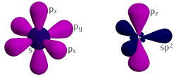
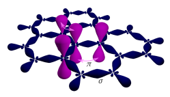
Three of the four outer-shell electrons of each atom in a graphene sheet occupy three sp2 hybrid orbitals – a combination of orbitals s, px and py — that are shared with the three nearest atoms, forming σ-bonds. The length of these bonds is about 0.142 nanometers.[54][55]
The remaining outer-shell electron occupies a pz orbital that is oriented perpendicularly to the plane. These orbitals hybridize together to form two half-filled bands of free-moving electrons, π and π∗, which are responsible for most of graphene's notable electronic properties.[54] Recent quantitative estimates of aromatic stabilization and limiting size derived from the enthalpies of hydrogenation (ΔHhydro) agree well with the literature reports.[56]
Graphene sheets stack to form graphite with an interplanar spacing of 0.335 nm (3.35 Å).
Graphene sheets in solid form usually show evidence in diffraction for graphite's (002) layering. This is true of some single-walled nanostructures.[57] However, unlayered graphene with only (hk0) rings has been found in the core of presolar graphite onions.[58] TEM studies show faceting at defects in flat graphene sheets[59] and suggest a role for two-dimensional crystallization from a melt.
Geometry edit
The hexagonal lattice structure of isolated, single-layer graphene can be directly seen with transmission electron microscopy (TEM) of sheets of graphene suspended between bars of a metallic grid[35] Some of these images showed a "rippling" of the flat sheet, with amplitude of about one nanometer. These ripples may be intrinsic to the material as a result of the instability of two-dimensional crystals,[2][60][61] or may originate from the ubiquitous dirt seen in all TEM images of graphene. Photoresist residue, which must be removed to obtain atomic-resolution images, may be the "adsorbates" observed in TEM images, and may explain the observed rippling.[citation needed]
The hexagonal structure is also seen in scanning tunneling microscope (STM) images of graphene supported on silicon dioxide substrates[62] The rippling seen in these images is caused by conformation of graphene to the subtrate's lattice, and is not intrinsic.[62]
Stability edit
Ab initio calculations show that a graphene sheet is thermodynamically unstable if its size is less than about 20 nm and becomes the most stable fullerene (as within graphite) only for molecules larger than 24,000 atoms.[63]
Properties edit
Electronic edit

Graphene is a zero-gap semiconductor, because its conduction and valence bands meet at the Dirac points. The Dirac points are six locations in momentum space, on the edge of the Brillouin zone, divided into two non-equivalent sets of three points. The two sets are labeled K and K'. The sets give graphene a valley degeneracy of gv = 2. By contrast, for traditional semiconductors the primary point of interest is generally Γ, where momentum is zero.[54] Four electronic properties separate it from other condensed matter systems.
However, if the in-plane direction is no longer infinite, but confined, its electronic structure would change. They are referred to as graphene nanoribbons. If it is "zig-zag", the bandgap would still be zero. If it is "armchair", the bandgap would be non-zero.
Graphene's hexagonal lattice can be regarded as two interleaving triangular lattices. This perspective was successfully used to calculate the band structure for a single graphite layer using a tight-binding approximation.[54]
Electronic spectrum edit
Electrons propagating through graphene's honeycomb lattice effectively lose their mass, producing quasi-particles that are described by a 2D analogue of the Dirac equation rather than the Schrödinger equation for spin-1/2 particles.[64][65]
Dispersion relation edit
The cleavage technique led directly to the first observation of the anomalous quantum Hall effect in graphene in 2005, by Geim's group and by Philip Kim and Yuanbo Zhang. This effect provided direct evidence of graphene's theoretically predicted Berry's phase of massless Dirac fermions and the first proof of the Dirac fermion nature of electrons.[31][33] These effects had been observed in bulk graphite by Yakov Kopelevich, Igor A. Luk'yanchuk, and others, in 2003–2004.[66][67]
When the atoms are placed onto the graphene hexagonal lattice, the overlap between the pz(π) orbitals and the s or the px and py orbitals is zero by symmetry. The pz electrons forming the π bands in graphene can therefore be treated independently. Within this π-band approximation, using a conventional tight-binding model, the dispersion relation (restricted to first-nearest-neighbor interactions only) that produces energy of the electrons with wave vector k is[29][68]

with the nearest-neighbor (π orbitals) hopping energy γ0 ≈ 2.8 eV and the lattice constant a ≈ 2.46 Å. The conduction and valence bands, respectively, correspond to the different signs. With one pz electron per atom in this model the valence band is fully occupied, while the conduction band is vacant. The two bands touch at the zone corners (the K point in the Brillouin zone), where there is a zero density of states but no band gap. The graphene sheet thus displays a semimetallic (or zero-gap semiconductor) character, although the same cannot be said of a graphene sheet rolled into a carbon nanotube, due to its curvature. Two of the six Dirac points are independent, while the rest are equivalent by symmetry. In the vicinity of the K-points the energy depends linearly on the wave vector, similar to a relativistic particle.[29][69] Since an elementary cell of the lattice has a basis of two atoms, the wave function has an effective 2-spinor structure.
As a consequence, at low energies, even neglecting the true spin, the electrons can be described by an equation that is formally equivalent to the massless Dirac equation. Hence, the electrons and holes are called Dirac fermions.[29] This pseudo-relativistic description is restricted to the chiral limit, i.e., to vanishing rest mass M0, which leads to interesting additional features:[29][70]

Here vF ~ 106 m/s (.003 c) is the Fermi velocity in graphene, which replaces the velocity of light in the Dirac theory; is the vector of the Pauli matrices, is the two-component wave function of the electrons, and E is their energy.[64]


The equation describing the electrons' linear dispersion relation is

where the wavevector q is measured from the Brillouin zone vertex K, , and the zero of energy is set to coincide with the Dirac point. The equation uses a pseudospin matrix formula that describes two sublattices of the honeycomb lattice.[69]

Single-atom wave propagation edit
Electron waves in graphene propagate within a single-atom layer, making them sensitive to the proximity of other materials such as high-κ dielectrics, superconductors and ferromagnetics.
Ambipolar electron and hole transport edit

Graphene displays remarkable electron mobility at room temperature, with reported values in excess of 15000 cm2⋅V−1⋅s−1.[2] Hole and electron mobilities are nearly the same.[65] The mobility is independent of temperature between 10 K and 100 K,[31][71][72] and shows little change even at room temperature (300 K),[2] which implies that the dominant scattering mechanism is defect scattering. Scattering by graphene's acoustic phonons intrinsically limits room temperature mobility in freestanding graphene to 200000 cm2⋅V−1⋅s−1 at a carrier density of 1012 cm−2.[72][73]
The corresponding resistivity of graphene sheets would be 10−8 Ω⋅m. This is less than the resistivity of silver, the lowest otherwise known at room temperature.[74] However, on SiO
2 substrates, scattering of electrons by optical phonons of the substrate is a larger effect than scattering by graphene's own phonons. This limits mobility to 40000 cm2⋅V−1⋅s−1.[72]
Charge transport has major concerns due to adsorption of contaminants such as water and oxygen molecules. This leads to non-repetitive and large hysteresis I-V characteristics. Researchers must carry out electrical measurements in vacuum. The protection of graphene surface by a coating with materials such as SiN, PMMA, h-BN, etc., have been discussed by researchers. In January 2015, the first stable graphene device operation in air over several weeks was reported, for graphene whose surface was protected by aluminum oxide.[75][76] In 2015, lithium-coated graphene exhibited superconductivity, a first for graphene.[77]
Electrical resistance in 40-nanometer-wide nanoribbons of epitaxial graphene changes in discrete steps. The ribbons' conductance exceeds predictions by a factor of 10. The ribbons can act more like optical waveguides or quantum dots, allowing electrons to flow smoothly along the ribbon edges. In copper, resistance increases in proportion to length as electrons encounter impurities.[78][79]
Transport is dominated by two modes. One is ballistic and temperature-independent, while the other is thermally activated. Ballistic electrons resemble those in cylindrical carbon nanotubes. At room temperature, resistance increases abruptly at a particular length—the ballistic mode at 16 micrometres and the other at 160 nanometres (1% of the former length).[78]
Graphene electrons can cover micrometer distances without scattering, even at room temperature.[64]
Despite zero carrier density near the Dirac points, graphene exhibits a minimum conductivity on the order of . The origin of this minimum conductivity is still unclear. However, rippling of the graphene sheet or ionized impurities in the SiO
2 substrate may lead to local puddles of carriers that allow conduction.[65] Several theories suggest that the minimum conductivity should be ; however, most measurements are of order or greater[2] and depend on impurity concentration.[80]


Near zero carrier density graphene exhibits positive photoconductivity and negative photoconductivity at high carrier density. This is governed by the interplay between photoinduced changes of both the Drude weight and the carrier scattering rate.[81]
Graphene doped with various gaseous species (both acceptors and donors) can be returned to an undoped state by gentle heating in vacuum.[80][82] Even for dopant concentrations in excess of 1012 cm−2 carrier mobility exhibits no observable change.[82] Graphene doped with potassium in ultra-high vacuum at low temperature can reduce mobility 20-fold.[80][83] The mobility reduction is reversible on heating the graphene to remove the potassium.
Due to graphene's two dimensions, charge fractionalization (where the apparent charge of individual pseudoparticles in low-dimensional systems is less than a single quantum[84]) is thought to occur. It may therefore be a suitable material for constructing quantum computers[85] using anyonic circuits.[86]
Chiral half-integer quantum Hall effect edit

The quantum Hall effect is a quantum mechanical version of the Hall effect, which is the production of transverse (perpendicular to the main current) conductivity in the presence of a magnetic field. The quantization of the Hall effect at integer multiples (the "Landau level") of the basic quantity e2/h (where e is the elementary electric charge and h is the Planck constant). It can usually be observed only in very clean silicon or gallium arsenide solids at temperatures around 3 K and very high magnetic fields.

Graphene shows the quantum Hall effect with respect to conductivity quantization: the effect is unordinary in that the sequence of steps is shifted by 1/2 with respect to the standard sequence and with an additional factor of 4. Graphene's Hall conductivity is , where N is the Landau level and the double valley and double spin degeneracies give the factor of 4.[2] These anomalies are present not only at extremely low temperatures but also at room temperature, i.e. at roughly 20 °C (293 K).[31]

This behavior is a direct result of graphene's chiral, massless Dirac electrons.[2][87] In a magnetic field, their spectrum has a Landau level with energy precisely at the Dirac point. This level is a consequence of the Atiyah–Singer index theorem and is half-filled in neutral graphene,[29] leading to the "+1/2" in the Hall conductivity.[32] Bilayer graphene also shows the quantum Hall effect, but with only one of the two anomalies (i.e. ). In the second anomaly, the first plateau at N = 0 is absent, indicating that bilayer graphene stays metallic at the neutrality point.[2]


Unlike normal metals, graphene's longitudinal resistance shows maxima rather than minima for integral values of the Landau filling factor in measurements of the Shubnikov–de Haas oscillations, whereby the term integral quantum Hall effect. These oscillations show a phase shift of π, known as Berry's phase.[31][65] Berry's phase arises due to chirality or dependence (locking) of the pseudospin quantum number on momentum of low-energy electrons near the Dirac points.[33] The temperature dependence of the oscillations reveals that the carriers have a non-zero cyclotron mass, despite their zero effective mass in the Dirac-fermion formalism.[31]
Graphene samples prepared on nickel films, and on both the silicon face and carbon face of silicon carbide, show the anomalous effect directly in electrical measurements.[88][89][90][91][92][93] Graphitic layers on the carbon face of silicon carbide show a clear Dirac spectrum in angle-resolved photoemission experiments, and the effect is observed in cyclotron resonance and tunneling experiments.[94]
Strong magnetic fields edit
In magnetic fields above 10 tesla or so additional plateaus of the Hall conductivity at σxy = νe2/h with ν = 0, ±1, ±4 are observed.[95] A plateau at ν = 3[96] and the fractional quantum Hall effect at ν = 1/3 were also reported.[96][97]
These observations with ν = 0, ±1, ±3, ±4 indicate that the four-fold degeneracy (two valley and two spin degrees of freedom) of the Landau energy levels is partially or completely lifted.
Casimir effect edit
The Casimir effect is an interaction between disjoint neutral bodies provoked by the fluctuations of the electrodynamical vacuum. Mathematically it can be explained by considering the normal modes of electromagnetic fields, which explicitly depend on the boundary (or matching) conditions on the interacting bodies' surfaces. Since graphene/electromagnetic field interaction is strong for a one-atom-thick material, the Casimir effect is of growing interest.[98][99]
Van der Waals force edit
The Van der Waals force (or dispersion force) is also unusual, obeying an inverse cubic, asymptotic power law in contrast to the usual inverse quartic.[100]
'Massive' electrons edit
Graphene's unit cell has two identical carbon atoms and two zero-energy states: one in which the electron resides on atom A, the other in which the electron resides on atom B. However, if the two atoms in the unit cell are not identical, the situation changes. Hunt et al. show that placing hexagonal boron nitride (h-BN) in contact with graphene can alter the potential felt at atom A versus atom B enough that the electrons develop a mass and accompanying band gap of about 30 meV [0.03 Electron Volt(eV)].[101]
The mass can be positive or negative. An arrangement that slightly raises the energy of an electron on atom A relative to atom B gives it a positive mass, while an arrangement that raises the energy of atom B produces a negative electron mass. The two versions behave alike and are indistinguishable via optical spectroscopy. An electron traveling from a positive-mass region to a negative-mass region must cross an intermediate region where its mass once again becomes zero. This region is gapless and therefore metallic. Metallic modes bounding semiconducting regions of opposite-sign mass is a hallmark of a topological phase and display much the same physics as topological insulators.[101]
If the mass in graphene can be controlled, electrons can be confined to massless regions by surrounding them with massive regions, allowing the patterning of quantum dots, wires, and other mesoscopic structures. It also produces one-dimensional conductors along the boundary. These wires would be protected against backscattering and could carry currents without dissipation.[101]
Permittivity edit
Graphene's permittivity varies with frequency. Over a range from microwave to millimeter wave frequencies it is roughly 3.3.[102] This permittivity, combined with the ability to form both conductors and insulators, means that theoretically, compact capacitors made of graphene could store large amounts of electrical energy.
Optical edit
Graphene's unique optical properties produce an unexpectedly high opacity for an atomic monolayer in vacuum, absorbing πα ≈ 2.3% of light, from visible to infrared.[8][9][103] Here, α is the fine-structure constant. This is a consequence of the "unusual low-energy electronic structure of monolayer graphene that features electron and hole conical bands meeting each other at the Dirac point... [which] is qualitatively different from more common quadratic massive bands."[8] Based on the Slonczewski–Weiss–McClure (SWMcC) band model of graphite, the interatomic distance, hopping value and frequency cancel when optical conductance is calculated using Fresnel equations in the thin-film limit.
Although confirmed experimentally, the measurement is not precise enough to improve on other techniques for determining the fine-structure constant.[104]
Multi-Parametric Surface Plasmon Resonance was used to characterize both thickness and refractive index of chemical-vapor-deposition (CVD)-grown graphene films. The measured refractive index and extinction coefficient values at 670 nm (6.7×10⁻⁷ m) wavelength are 3.135 and 0.897, respectively. The thickness was determined as 3.7Å from a 0.5mm area, which agrees with 3.35Å reported for layer-to-layer carbon atom distance of graphite crystals.[105] The method can be further used also for real-time label-free interactions of graphene with organic and inorganic substances. Furthermore, the existence of unidirectional surface plasmons in the nonreciprocal graphene-based gyrotropic interfaces has been demonstrated theoretically. By efficiently controlling the chemical potential of graphene, the unidirectional working frequency can be continuously tunable from THz to near-infrared and even visible.[106] Particularly, the unidirectional frequency bandwidth can be 1– 2 orders of magnitude larger than that in metal under the same magnetic field, which arises from the superiority of extremely small effective electron mass in graphene.
Graphene's band gap can be tuned from 0 to 0.25 eV (about 5 micrometre wavelength) by applying voltage to a dual-gate bilayer graphene field-effect transistor (FET) at room temperature.[107] The optical response of graphene nanoribbons is tunable into the terahertz regime by an applied magnetic field.[108] Graphene/graphene oxide systems exhibit electrochromic behavior, allowing tuning of both linear and ultrafast optical properties.[109]
A graphene-based Bragg grating (one-dimensional photonic crystal) has been fabricated and demonstrated its capability for excitation of surface electromagnetic waves in the periodic structure by using 633 nm (6.33×10⁻⁷ m) He–Ne laser as the light source.[110]
Saturable absorption edit
Such unique absorption could become saturated when the input optical intensity is above a threshold value. This nonlinear optical behavior is termed saturable absorption and the threshold value is called the saturation fluence. Graphene can be saturated readily under strong excitation over the visible to near-infrared region, due to the universal optical absorption and zero band gap. This has relevance for the mode locking of fiber lasers, where fullband mode locking has been achieved by graphene-based saturable absorber. Due to this special property, graphene has wide application in ultrafast photonics. Moreover, the optical response of graphene/graphene oxide layers can be tuned electrically.[109][111][112][113][114][115]
Saturable absorption in graphene could occur at the Microwave and Terahertz band, owing to its wideband optical absorption property. The microwave saturable absorption in graphene demonstrates the possibility of graphene microwave and terahertz photonics devices, such as a microwave saturable absorber, modulator, polarizer, microwave signal processing and broad-band wireless access networks.[116]
Nonlinear Kerr effect edit
Under more intensive laser illumination, graphene could also possess a nonlinear phase shift due to the optical nonlinear Kerr effect. Based on a typical open and close aperture z-scan measurement, graphene possesses a giant nonlinear Kerr coefficient of 10−7 cm2⋅W−1, almost nine orders of magnitude larger than that of bulk dielectrics.[117] This suggests that graphene may be a powerful nonlinear Kerr medium, with the possibility of observing a variety of nonlinear effects, the most important of which is the soliton.[118]
Excitonic edit
First-principle calculations with quasiparticle corrections and many-body effects are performed to study the electronic and optical properties of graphene-based materials. The approach is described as three stages.[119] With GW calculation, the properties of graphene-based materials are accurately investigated, including bulk graphene,[120] nanoribbons,[121] edge and surface functionalized armchair oribbons,[122] hydrogen saturated armchair ribbons,[123] Josephson effect in graphene SNS junctions with single localized defect[124] and armchair ribbon scaling properties.[125]
Spin transport edit
Graphene is claimed to be an ideal material for spintronics due to its small spin–orbit interaction and the near absence of nuclear magnetic moments in carbon (as well as a weak hyperfine interaction). Electrical spin current injection and detection has been demonstrated up to room temperature.[126][127][128] Spin coherence length above 1 micrometre at room temperature was observed,[126] and control of the spin current polarity with an electrical gate was observed at low temperature.[127]
Magnetic properties edit
Strong magnetic fields edit
Graphene's quantum Hall effect in magnetic fields above approximately 10 Teslas reveals additional interesting features. Additional plateaus of the Hall conductivity at with are observed.[95] Also, the observation of a plateau at [96] and the fractional quantum Hall effect at were reported.[96][97]


These observations with indicate that the four-fold degeneracy (two valley and two spin degrees of freedom) of the Landau energy levels is partially or completely lifted. One hypothesis is that the magnetic catalysis of symmetry breaking is responsible for lifting the degeneracy.[citation needed]

Spintronic and magnetic properties can be present in graphene simultaneously.[129] Low-defect graphene nanomeshes manufactured by using a non-lithographic method exhibit large-amplitude ferromagnetism even at room temperature. Additionally a spin pumping effect is found for fields applied in parallel with the planes of few-layer ferromagnetic nanomeshes, while a magnetoresistance hysteresis loop is observed under perpendicular fields. Charge-neutral graphene has been shown to exhibit magnetoresistance above 100% in magnetic fields of standard permanent magnets (about 0.1 tesla), a record magnetoresistivity at room temperature among all known materials.[130]
Magnetic substrates edit
In 2014 researchers magnetized graphene by placing it on an atomically smooth layer of magnetic yttrium iron garnet. The graphene's electronic properties were unaffected. Prior approaches involved doping graphene with other substances.[131] The dopant's presence negatively affected its electronic properties.[132]
Thermal conductivity edit
Thermal transport in graphene is an active area of research, which has attracted attention because of the potential for thermal management applications. Most experimental measurements have posted large uncertainties in the results of thermal conductivity due to limitations of the instruments used. Following predictions for graphene and related carbon nanotubes,[133] early measurements of the thermal conductivity of suspended graphene reported an exceptionally large thermal conductivity up to 5300 W⋅m−1⋅K−1,[134] compared with the thermal conductivity of pyrolytic graphite of approximately 2000 W⋅m−1⋅K−1 at room temperature.[135] However, later studies primarily on more scalable but more defected graphene derived by Chemical Vapor Deposition have been unable to reproduce such high thermal conductivity measurements, producing a wide range of thermal conductivities between 1500 – 2500 W⋅m−1⋅K−1 for suspended single layer graphene.[136][137][138][139] The large range in the reported thermal conductivity can be caused by large measurement uncertainties as well as variations in the graphene quality and processing conditions. In addition, it is known that when single-layer graphene is supported on an amorphous material, the thermal conductivity is reduced to about 500 – 600 W⋅m−1⋅K−1 at room temperature as a result of scattering of graphene lattice waves by the substrate,[140][141] and can be even lower for few layer graphene encased in amorphous oxide.[142] Likewise, polymeric residue can contribute to a similar decrease in the thermal conductivity of suspended graphene to approximately 500 – 600 W⋅m−1⋅K−1 for bilayer graphene.[143]
It has been suggested that the isotopic composition, the ratio of 12C to 13C, has a significant impact on the thermal conductivity. For example, isotopically pure 12C graphene has higher thermal conductivity than either a 50:50 isotope ratio or the naturally occurring 99:1 ratio.[144] It can be shown by using the Wiedemann–Franz law, that the thermal conduction is phonon-dominated.[134] However, for a gated graphene strip, an applied gate bias causing a Fermi energy shift much larger than kBT can cause the electronic contribution to increase and dominate over the phonon contribution at low temperatures. The ballistic thermal conductance of graphene is isotropic.[145][146]
Potential for this high conductivity can be seen by considering graphite, a 3D version of graphene that has basal plane thermal conductivity of over a 1000 W⋅m−1⋅K−1 (comparable to diamond). In graphite, the c-axis (out of plane) thermal conductivity is over a factor of ~100 smaller due to the weak binding forces between basal planes as well as the larger lattice spacing.[147] In addition, the ballistic thermal conductance of graphene is shown to give the lower limit of the ballistic thermal conductances, per unit circumference, length of carbon nanotubes.[148]
Despite its 2-D nature, graphene has 3 acoustic phonon modes. The two in-plane modes (LA, TA) have a linear dispersion relation, whereas the out of plane mode (ZA) has a quadratic dispersion relation. Due to this, the T2 dependent thermal conductivity contribution of the linear modes is dominated at low temperatures by the T1.5 contribution of the out of plane mode.[148] Some graphene phonon bands display negative Grüneisen parameters.[149] At low temperatures (where most optical modes with positive Grüneisen parameters are still not excited) the contribution from the negative Grüneisen parameters will be dominant and thermal expansion coefficient (which is directly proportional to Grüneisen parameters) negative. The lowest negative Grüneisen parameters correspond to the lowest transverse acoustic ZA modes. Phonon frequencies for such modes increase with the in-plane lattice parameter since atoms in the layer upon stretching will be less free to move in the z direction. This is similar to the behavior of a string, which, when it is stretched, will have vibrations of smaller amplitude and higher frequency. This phenomenon, named "membrane effect," was predicted by Lifshitz in 1952.[150]
Mechanical edit
The (two-dimensional) density of graphene is 0.763 mg per square meter.[citation needed]
Graphene is the strongest material ever tested,[10][11] with an intrinsic tensile strength of 130 GPa (19,000,000 psi) (with representative engineering tensile strength ~50-60 GPa for stretching large-area freestanding graphene) and a Young's modulus (stiffness) close to 1 TPa (150,000,000 psi). The Nobel announcement illustrated this by saying that a 1 square meter graphene hammock would support a 4 kg cat but would weigh only as much as one of the cat's whiskers, at 0.77 mg (about 0.001% of the weight of 1 m2 of paper).[151]
Large-angle-bent graphene monolayer has been achieved with negligible strain, showing mechanical robustness of the two-dimensional carbon nanostructure. Even with extreme deformation, excellent carrier mobility in monolayer graphene can be preserved.[152]
The spring constant of suspended graphene sheets has been measured using an atomic force microscope (AFM). Graphene sheets were suspended over SiO
2 cavities where an AFM tip was used to apply a stress to the sheet to test its mechanical properties. Its spring constant was in the range 1–5 N/m and the stiffness was 0.5 TPa, which differs from that of bulk graphite. These intrinsic properties could lead to applications such as NEMS as pressure sensors and resonators.[153] Due to its large surface energy and out of plane ductility, flat graphene sheets are unstable with respect to scrolling, i.e. bending into a cylindrical shape, which is its lower-energy state.[154]
As is true of all materials, regions of graphene are subject to thermal and quantum fluctuations in relative displacement. Although the amplitude of these fluctuations is bounded in 3D structures (even in the limit of infinite size), the Mermin–Wagner theorem shows that the amplitude of long-wavelength fluctuations grows logarithmically with the scale of a 2D structure, and would therefore be unbounded in structures of infinite size. Local deformation and elastic strain are negligibly affected by this long-range divergence in relative displacement. It is believed that a sufficiently large 2D structure, in the absence of applied lateral tension, will bend and crumple to form a fluctuating 3D structure. Researchers have observed ripples in suspended layers of graphene,[35] and it has been proposed that the ripples are caused by thermal fluctuations in the material. As a consequence of these dynamical deformations, it is debatable whether graphene is truly a 2D structure.[2][60][61][155][156] It has recently been shown that these ripples, if amplified through the introduction of vacancy defects, can impart a negative Poisson's ratio into graphene, resulting in the thinnest auxetic material known so far.[157]
Graphene nanosheets have been incorporated into a Ni matrix through a plating process to form Ni-graphene composites on a target substrate. The enhancement in mechanical properties of the composites is attributed to the high interaction between Ni and graphene and the prevention of the dislocation sliding in the Ni matrix by the graphene.[158]
Fracture toughness edit
In 2014, researchers from Rice University and the Georgia Institute of Technology have indicated that despite its strength, graphene is also relatively brittle, with a fracture toughness of about 4 MPa√m.[159] This indicates that imperfect graphene is likely to crack in a brittle manner like ceramic materials, as opposed to many metallic materials which tend to have fracture toughnesses in the range of 15–50 MPa√m. Later in 2014, the Rice team announced that graphene showed a greater ability to distribute force from an impact than any known material, ten times that of steel per unit weight.[160] The force was transmitted at 22.2 kilometres per second (13.8 mi/s).[161]
Polycrystalline graphene edit
Various methods – most notably, chemical vapor deposition (CVD), as discussed in the section below - have been developed to produce large-scale graphene needed for device applications. Such methods often synthesize polycrystalline graphene.[162] The mechanical properties of polycrystalline graphene is affected by the nature of the defects, such as grain-boundaries (GB) and vacancies, present in the system and the average grain-size.
Graphene grain boundaries typically contain heptagon-pentagon pairs. The arrangement of such defects depends on whether the GB is in zig-zag or armchair direction. It further depends on the tilt-angle of the GB.[163] In 2010, researchers from Brown University computationally predicted that as the tilt-angle increases, the grain boundary strength also increases. They showed that the weakest link in the grain boundary is at the critical bonds of the heptagon rings. As the grain boundary angle increases, the strain in these heptagon rings decreases, causing the grain-boundary to be stronger than lower-angle GBs. They proposed that, in fact, for sufficiently large angle GB, the strength of the GB is similar to pristine graphene.[164] In 2012, it was further shown that the strength can increase or decrease, depending on the detailed arrangements of the defects.[165] These predictions have since been supported by experimental evidences. In a 2013 study led by James Hone's group, researchers probed the elastic stiffness and strength of CVD-grown graphene by combining nano-indentation and high-resolution TEM. They found that the elastic stiffness is identical and strength is only slightly lower than those in pristine graphene.[166] In the same year, researchers from UC Berkeley and UCLA probed bi-crystalline graphene with TEM and AFM. They found that the strength of grain-boundaries indeed tend to increase with the tilt angle.[167]
While the presence of vacancies is not only prevalent in polycrystalline graphene, vacancies can have significant effects on the strength of graphene. The general consensus is that the strength decreases along with increasing densities of vacancies. In fact, various studies have shown that for graphene with sufficiently low density of vacancies, the strength does not vary significantly from that of pristine graphene. On the other hand, high density of vacancies can severely reduce the strength of graphene.[168]
Compared to the fairly well-understood nature of the effect that grain boundary and vacancies have on the mechanical properties of graphene, there is no clear consensus on the general effect that the average grain size has on the strength of polycrystalline graphene.[169][168][170] In fact, three notable theoretical/computational studies on this topic have led to three different conclusions.[171][172][173] First, in 2012, Kotakoski and Myer studied the mechanical properties of polycrystalline graphene with "realistic atomistic model", using molecular-dynamics (MD) simulation. To emulate the growth mechanism of CVD, they first randomly selected nucleation sites that are at least 5A (arbitrarily chosen) apart from other sites. Polycrystalline graphene was generated from these nucleation sites and was subsequently annealed at 3000K, then quenched. Based on this model, they found that cracks are initiated at grain-boundary junctions, but the grain size does not significantly affect the strength.[171] Second, in 2013, Z. Song et al. used MD simulations to study the mechanical properties of polycrystalline graphene with uniform-sized hexagon-shaped grains. The hexagon grains were oriented in various lattice directions and the GBs consisted of only heptagon, pentagon, and hexagonal carbon rings. The motivation behind such model was that similar systems had been experimentally observed in graphene flakes grown on the surface of liquid copper. While they also noted that crack is typically initiated at the triple junctions, they found that as the grain size decreases, the yield strength of graphene increases. Based on this finding, they proposed that polycrystalline follows pseudo Hall-Petch relationship.[172] Third, in 2013, Z. D. Sha et al. studied the effect of grain size on the properties of polycrystalline graphene, by modelling the grain patches using Voronoi construction. The GBs in this model consisted of heptagon, pentagon, and hexagon, as well as squares, octagons, and vacancies. Through MD simulation, contrary to the fore-mentioned study, they found inverse Hall-Petch relationship, where the strength of graphene increases as the grain size increases.[173] Experimental observations and other theoretical predictions also gave differing conclusions, similar to the three given above.[170] Such discrepancies show the complexity of the effects that grain size, arrangements of defects, and the nature of defects have on the mechanical properties of polycrystalline graphene.
Chemical edit
Graphene has a theoretical specific surface area (SSA) of 2630 m2/g. This is much larger than that reported to date for carbon black (typically smaller than 900 m2/g) or for carbon nanotubes (CNTs), from ≈100 to 1000 m2/g and is similar to activated carbon.[174] Graphene is the only form of carbon (or solid material) in which every atom is available for chemical reaction from two sides (due to the 2D structure). Atoms at the edges of a graphene sheet have special chemical reactivity. Graphene has the highest ratio of edge atoms of any allotrope. Defects within a sheet increase its chemical reactivity.[175] The onset temperature of reaction between the basal plane of single-layer graphene and oxygen gas is below 260 °C (530 K).[176] Graphene burns at very low temperature (e.g., 350 °C (620 K)).[177] Graphene is commonly modified with oxygen- and nitrogen-containing functional groups and analyzed by infrared spectroscopy and X-ray photoelectron spectroscopy. However, determination of structures of graphene with oxygen-[178] and nitrogen-[179] functional groups requires the structures to be well controlled.
In 2013, Stanford University physicists reported that single-layer graphene is a hundred times more chemically reactive than thicker multilayer sheets.[180]
Graphene can self-repair holes in its sheets, when exposed to molecules containing carbon, such as hydrocarbons. Bombarded with pure carbon atoms, the atoms perfectly align into hexagons, completely filling the holes.[181][182]
Biological edit
Despite the promising results in different cell studies and proof of concept studies, there is still incomplete understanding of the full biocompatibility of graphene based materials.[183] Different cell lines react differently when exposed to graphene, and it has been shown that the lateral size of the graphene flakes, the form and surface chemistry can elicit different biological responses on the same cell line.[184]
There are indications that graphene has promise as a useful material for interacting with neural cells; studies on cultured neural cells show limited success.[185][186]
Graphene also has some utility in osteogenics. Researchers at the Graphene Research Centre at the National University of Singapore (NUS) discovered in 2011 the ability of graphene to accelerate the osteogenic differentiation of human Mesenchymal Stem Cells without the use of biochemical inducers.[187]
Graphene can be used in biosensors; in 2015, researchers demonstrated that a graphene-based sensor be can used to detect a cancer risk biomarker. In particular, by using epitaxial graphene on silicon carbide, they were repeatably able to detect 8-hydroxydeoxyguanosine (8-OHdG), a DNA damage biomarker.[188]
Support substrate edit
The electronics property of graphene can be significantly influenced by the supporting substrate. Studies of graphene monolayers on clean and hydrogen(H)-passivated silicon (100) (Si(100)/H) surfaces have been performed.[189] The Si(100)/H surface does not perturb the electronic properties of graphene, whereas the interaction between the clean Si(100) surface and graphene changes the electronic states of graphene significantly. This effect results from the covalent bonding between C and surface Si atoms, modifying the π-orbital network of the graphene layer. The local density of states shows that the bonded C and Si surface states are highly disturbed near the Fermi energy.
Forms edit
Monolayer sheets edit
In 2013 a group of Polish scientists presented a production unit that allows the manufacture of continuous monolayer sheets.[190] The process is based on graphene growth on a liquid metal matrix.[191] The product of this process was called High Strength Metallurgical Graphene. In a new study published in Nature, the researchers have used a single layer graphene electrode and a novel surface sensitive non-linear spectroscopy technique to investigate the top-most water layer at the electrochemically charged surface. They found that the interfacial water response to applied electric field is asymmetric with respect to the nature of the applied field.[192]
Bilayer graphene edit
Bilayer graphene displays the anomalous quantum Hall effect, a tunable band gap[193] and potential for excitonic condensation[194] –making it a promising candidate for optoelectronic and nanoelectronic applications. Bilayer graphene typically can be found either in twisted configurations where the two layers are rotated relative to each other or graphitic Bernal stacked configurations where half the atoms in one layer lie atop half the atoms in the other.[195] Stacking order and orientation govern the optical and electronic properties of bilayer graphene.
One way to synthesize bilayer graphene is via chemical vapor deposition, which can produce large bilayer regions that almost exclusively conform to a Bernal stack geometry.[195]
It has been shown that the two graphene layers can withstand important strain or doping mismatch[196] which ultimately should lead to their exfoliation.
Turbostratic edit
Turbostratic graphene exhibits weak interlayer coupling, and the spacing is increased with respect to Bernal-stacked multilayer graphene. Rotational misalignment preserves the 2D electronic structure, as confirmed by Raman spectroscopy. The D peak is very weak, whereas the 2D and G peaks remain prominent. A rather peculiar feature is that the I2D/IG ratio can exceed 10. However, most importantly, the M peak, which originates from AB stacking, is absent, whereas the TS1 and TS2 modes are visible in the Raman spectrum.[197][198] The material is formed through conversion of non-graphenic carbon into graphenic carbon without providing sufficient energy to allow for the reorganization through annealing of adjacent graphene layers into crystalline graphitic structures.
Graphene superlattices edit
Periodically stacked graphene and its insulating isomorph provide a fascinating structural element in implementing highly functional superlattices at the atomic scale, which offers possibilities in designing nanoelectronic and photonic devices. Various types of superlattices can be obtained by stacking graphene and its related forms.[199] The energy band in layer-stacked superlattices is found to be more sensitive to the barrier width than that in conventional III–V semiconductor superlattices. When adding more than one atomic layer to the barrier in each period, the coupling of electronic wavefunctions in neighboring potential wells can be significantly reduced, which leads to the degeneration of continuous subbands into quantized energy levels. When varying the well width, the energy levels in the potential wells along the L-M direction behave distinctly from those along the K-H direction.
A superlattice corresponds to a periodic or quasi-periodic arrangement of different materials, and can be described by a superlattice period which confers a new translational symmetry to the system, impacting their phonon dispersions and subsequently their thermal transport properties. Recently, uniform monolayer graphene-hBN structures have been successfully synthesized via lithography patterning coupled with chemical vapor deposition (CVD).[200] Furthermore, superlattices of graphene-hBN are ideal model systems for the realization and understanding of coherent (wave-like) and incoherent (particle-like) phonon thermal transport.[201][202][203][204][205]
Graphene nanoribbons edit


Graphene nanoribbons ("nanostripes" in the "zig-zag"/"zigzag" orientation), at low temperatures, show spin-polarized metallic edge currents, which also suggests applications in the new field of spintronics. (In the "armchair" orientation, the edges behave like semiconductors.[64])
Graphene quantum dots edit
A graphene quantum dot (GQD) is a graphene fragment with size less than 100 nm. The properties of GQDs are different from 'bulk' graphene due to the quantum confinement effects which only becomes apparent when size is smaller than 100 nm.[206][207][208]
Graphene oxide edit
Graphene oxide is usually produced through chemical exfoliation of graphite. A particularly popular technique is the improved Hummer's method.[209] Using paper-making techniques on dispersed, oxidized and chemically processed graphite in water, the monolayer flakes form a single sheet and create strong bonds. These sheets, called graphene oxide paper, have a measured tensile modulus of 32 GPa.[210] The chemical property of graphite oxide is related to the functional groups attached to graphene sheets. These can change the polymerization pathway and similar chemical processes.[211] Graphene oxide flakes in polymers display enhanced photo-conducting properties.[212] Graphene is normally hydrophobic and impermeable to all gases and liquids (vacuum-tight). However, when formed into graphene oxide-based capillary membrane, both liquid water and water vapor flow through as quickly as if the membrane was not present.[213]
In 2022 were performed an avaluation of biological effects of graphene oxide [2]. It was shown the graphene oxide at low doses was evaluated for its biological effects on larvae and the imago of Drosophila melanogaster. Oral administration of graphene oxide at concentrations of 0.02-1% has a beneficial effect on the developmental rate and hatching ability of larvae. Long-term administration of a low dose of graphene oxide extends Drosophila lifespan and significantly enhances resistance to environmental stresses. These suggest about graphene oxide affects carbohydrate and lipid metabolism in adult Drosophila. These findings might provide a useful reference to assess the biological effects of graphene oxide, which could play an important role in a variety of graphene-based biomedical applications.[214]
Chemical modification edit

Soluble fragments of graphene can be prepared in the laboratory[215] through chemical modification of graphite. First, microcrystalline graphite is treated with an acidic mixture of sulfuric acid and nitric acid. A series of oxidation and exfoliation steps produce small graphene plates with carboxyl groups at their edges. These are converted to acid chloride groups by treatment with thionyl chloride; next, they are converted to the corresponding graphene amide via treatment with octadecylamine. The resulting material (circular graphene layers of 5.3 Å or 5.3×10⁻¹⁰ m thickness) is soluble in tetrahydrofuran, tetrachloromethane and dichloroethane.
Refluxing single-layer graphene oxide (SLGO) in solvents leads to size reduction and folding of individual sheets as well as loss of carboxylic group functionality, by up to 20%, indicating thermal instabilities of SLGO sheets dependent on their preparation methodology. When using thionyl chloride, acyl chloride groups result, which can then form aliphatic and aromatic amides with a reactivity conversion of around 70–80%.

Hydrazine reflux is commonly used for reducing SLGO to SLG(R), but titrations show that only around 20–30% of the carboxylic groups are lost, leaving a significant number available for chemical attachment. Analysis of SLG(R) generated by this route reveals that the system is unstable and using a room temperature stirring with HCl (< 1.0 M) leads to around 60% loss of COOH functionality. Room temperature treatment of SLGO with carbodiimides leads to the collapse of the individual sheets into star-like clusters that exhibited poor subsequent reactivity with amines (c. 3–5% conversion of the intermediate to the final amide).[216] It is apparent that conventional chemical treatment of carboxylic groups on SLGO generates morphological changes of individual sheets that leads to a reduction in chemical reactivity, which may potentially limit their use in composite synthesis. Therefore, chemical reactions types have been explored. SLGO has also been grafted with polyallylamine, cross-linked through epoxy groups. When filtered into graphene oxide paper, these composites exhibit increased stiffness and strength relative to unmodified graphene oxide paper.[217]
Full hydrogenation from both sides of graphene sheet results in graphane, but partial hydrogenation leads to hydrogenated graphene.[218] Similarly, both-side fluorination of graphene (or chemical and mechanical exfoliation of graphite fluoride) leads to fluorographene (graphene fluoride),[219] while partial fluorination (generally halogenation) provides fluorinated (halogenated) graphene.
Graphene ligand/complex edit
Graphene can be a ligand to coordinate metals and metal ions by introducing functional groups. Structures of graphene ligands are similar to e.g. metal-porphyrin complex, metal-phthalocyanine complex, and metal-phenanthroline complex. Copper and nickel ions can be coordinated with graphene ligands.[220][221]
Graphene fiber edit
In 2011, researchers reported a novel yet simple approach to fabricate graphene fibers from chemical vapor deposition grown graphene films.[222] The method was scalable and controllable, delivering tunable morphology and pore structure by controlling the evaporation of solvents with suitable surface tension. Flexible all-solid-state supercapacitors based on this graphene fibers were demonstrated in 2013.[223]
In 2015, intercalating small graphene fragments into the gaps formed by larger, coiled graphene sheets, after annealing provided pathways for conduction, while the fragments helped reinforce the fibers.[sentence fragment] The resulting fibers offered better thermal and electrical conductivity and mechanical strength. Thermal conductivity reached 1,290 W/m/K (1,290 watts per metre per kelvin), while tensile strength reached 1,080 MPa (157,000 psi).[224]
In 2016, Kilometer-scale continuous graphene fibers with outstanding mechanical properties and excellent electrical conductivity are produced by high-throughput wet-spinning of graphene oxide liquid crystals followed by graphitization through a full-scale synergetic defect-engineering strategy.[225] The graphene fibers with superior performances promise wide applications in functional textiles, lightweight motors, microelectronic devices, etc.
Tsinghua University in Beijing, led by Wei Fei of the Department of Chemical Engineering, claims to be able to create a carbon nanotube fibre which has a tensile strength of 80 GPa (12,000,000 psi).[226]
3D graphene edit
In 2013, a three-dimensional honeycomb of hexagonally arranged carbon was termed 3D graphene, and self-supporting 3D graphene was also produced.[227] 3D structures of graphene can be fabricated by using either CVD or solution based methods. A 2016 review by Khurram and Xu et al. provided a summary of then-state-of-the-art techniques for fabrication of the 3D structure of graphene and other related two-dimensional materials.[228] In 2013, researchers at Stony Brook University reported a novel radical-initiated crosslinking method to fabricate porous 3D free-standing architectures of graphene and carbon nanotubes using nanomaterials as building blocks without any polymer matrix as support.[229] These 3D graphene (all-carbon) scaffolds/foams have applications in several fields such as energy storage, filtration, thermal management and biomedical devices and implants.[228][230]
Box-shaped graphene (BSG) nanostructure appearing after mechanical cleavage of pyrolytic graphite was reported in 2016.[231] The discovered nanostructure is a multilayer system of parallel hollow nanochannels located along the surface and having quadrangular cross-section. The thickness of the channel walls is approximately equal to 1 nm. Potential fields of BSG application include: ultra-sensitive detectors, high-performance catalytic cells, nanochannels for DNA sequencing and manipulation, high-performance heat sinking surfaces, rechargeable batteries of enhanced performance, nanomechanical resonators, electron multiplication channels in emission nanoelectronic devices, high-capacity sorbents for safe hydrogen storage.
Three dimensional bilayer graphene has also been reported.[232][233]
Pillared graphene edit
Pillared graphene is a hybrid carbon, structure consisting of an oriented array of carbon nanotubes connected at each end to a sheet of graphene. It was first described theoretically by George Froudakis and colleagues of the University of Crete in Greece in 2008. Pillared graphene has not yet been synthesised in the laboratory, but it has been suggested that it may have useful electronic properties, or as a hydrogen storage material.
Reinforced graphene edit
Graphene reinforced with embedded carbon nanotube reinforcing bars ("rebar") is easier to manipulate, while improving the electrical and mechanical qualities of both materials.[234][235]
Functionalized single- or multiwalled carbon nanotubes are spin-coated on copper foils and then heated and cooled, using the nanotubes themselves as the carbon source. Under heating, the functional carbon groups decompose into graphene, while the nanotubes partially split and form in-plane covalent bonds with the graphene, adding strength. π–π stacking domains add more strength. The nanotubes can overlap, making the material a better conductor than standard CVD-grown graphene. The nanotubes effectively bridge the grain boundaries found in conventional graphene. The technique eliminates the traces of substrate on which later-separated sheets were deposited using epitaxy.[234]
Stacks of a few layers have been proposed as a cost-effective and physically flexible replacement for indium tin oxide (ITO) used in displays and photovoltaic cells.[234]
Moulded graphene edit
In 2015, researchers from the University of Illinois at Urbana-Champaign (UIUC) developed a new approach for forming 3D shapes from flat, 2D sheets of graphene.[236] A film of graphene that had been soaked in solvent to make it swell and become malleable was overlaid on an underlying substrate "former". The solvent evaporated over time, leaving behind a layer of graphene that had taken on the shape of the underlying structure. In this way they were able to produce a range of relatively intricate micro-structured shapes.[237] Features vary from 3.5 to 50 μm. Pure graphene and gold-decorated graphene were each successfully integrated with the substrate.[238]
Graphene aerogel edit
An aerogel made of graphene layers separated by carbon nanotubes was measured at 0.16 milligrams per cubic centimeter. A solution of graphene and carbon nanotubes in a mold is freeze dried to dehydrate the solution, leaving the aerogel. The material has superior elasticity and absorption. It can recover completely after more than 90% compression, and absorb up to 900 times its weight in oil, at a rate of 68.8 grams per second.[239]
Graphene nanocoil edit
In 2015, a coiled form of graphene was discovered in graphitic carbon (coal). The spiraling effect is produced by defects in the material's hexagonal grid that causes it to spiral along its edge, mimicking a Riemann surface, with the graphene surface approximately perpendicular to the axis. When voltage is applied to such a coil, current flows around the spiral, producing a magnetic field. The phenomenon applies to spirals with either zigzag or armchair patterns, although with different current distributions. Computer simulations indicated that a conventional spiral inductor of 205 microns in diameter could be matched by a nanocoil just 70 nanometers wide, with a field strength reaching as much as 1 tesla.[240]
The nano-solenoids analyzed through computer models at Rice should be capable of producing powerful magnetic fields of about 1 tesla, about the same as the coils found in typical loudspeakers, according to Yakobson and his team – and about the same field strength as some MRI machines. They found the magnetic field would be strongest in the hollow, nanometer-wide cavity at the spiral's center.[240]
A solenoid made with such a coil behaves as a quantum conductor whose current distribution between the core and exterior varies with applied voltage, resulting in nonlinear inductance.[241]
Crumpled graphene edit
In 2016, Brown University introduced a method for 'crumpling' graphene, adding wrinkles to the material on a nanoscale. This was achieved by depositing layers of graphene oxide onto a shrink film, then shrunken, with the film dissolved before being shrunken again on another sheet of film. The crumpled graphene became superhydrophobic, and, when used as a battery electrode, the material was shown to have as much as a 400% increase in electrochemical current density.[242][243]
Production edit
A rapidly increasing list of production techniques have been developed to enable graphene's use in commercial applications.[244]
Isolated 2D crystals cannot be grown via chemical synthesis beyond small sizes even in principle, because the rapid growth of phonon density with increasing lateral size forces 2D crystallites to bend into the third dimension. In all cases, graphene must bond to a substrate to retain its two-dimensional shape.[19]
Small graphene structures, such as graphene quantum dots and nanoribbons, can be produced by "bottom up" methods that assemble the lattice from organic molecule monomers (e. g. citric acid, glucose). "Top down" methods, on the other hand, cut bulk graphite and graphene materials with strong chemicals (e. g. mixed acids).
Mechanical edit
Mechanical exfoliation edit
Geim and Novoselov initially used adhesive tape to pull graphene sheets away from graphite. Achieving single layers typically requires multiple exfoliation steps. After exfoliation the flakes are deposited on a silicon wafer. Crystallites larger than 1 mm and visible to the naked eye can be obtained.[245]
As of 2014, exfoliation produced graphene with the lowest number of defects and highest electron mobility.[246]
Alternatively a sharp single-crystal diamond wedge penetrates onto the graphite source to cleave layers.[247]
In 2014 defect-free, unoxidized graphene-containing liquids were made from graphite using mixers that produce local shear rates greater than 10×104.[248][249]
Shear exfoliation is another method which by using rotor-stator mixer the scalable production of the defect-free Graphene has become possible.[250] It has been shown that, as turbulence is not necessary for mechanical exfoliation,[251] low speed ball milling is shown to be effective in the production of High-Yield and water-soluble graphene.
Liquid phase exfoliation edit
Liquid phase exfoliation (LPE) is a relatively simple method which involves dispersing graphite in a liquid medium to produce graphene by sonication or high shear mixing, followed by centrifugation.[252][253][254] Restacking is an issue with this technique unless solvents with appropriate surface energy are used (e.g. NMP).
Adding a surfactant to a solvent prior to sonication prevents restacking by adsorbing to the graphene's surface.[255] This produces a higher graphene concentration, but removing the surfactant requires chemical treatments.[citation needed]
LPE results in nanosheets with a broad size distribution and thicknesses roughly in the range of 1-10 monolayers. However, liquid cascade centrifugation can be used to size select the suspensions and achieve monolayer enrichment.[256]
Sonicating graphite at the interface of two immiscible liquids, most notably heptane and water, produced macro-scale graphene films. The graphene sheets are adsorbed to the high energy interface between the materials and are kept from restacking. The sheets are up to about 95% transparent and conductive.[257]
With definite cleavage parameters, the box-shaped graphene (BSG) nanostructure can be prepared on graphite crystal.[231]
A major advantage of LPE is that it can be used to exfoliate many inorganic 2D materials beyond graphene, e.g. BN, MoS2, WS2.[258]
Splitting monolayer carbon edit
Graphene can be created by opening carbon nanotubes by cutting or etching.[259] In one such method multi-walled carbon nanotubes are cut open in solution by action of potassium permanganate and sulfuric acid.[260][261]
In 2014, carbon nanotube-reinforced graphene was made via spin coating and annealing functionalized carbon nanotubes.[234]
Another approach sprays buckyballs at supersonic speeds onto a substrate. The balls cracked open upon impact, and the resulting unzipped cages then bond together to form a graphene film.[262]
Chemical edit
Graphite oxide reduction edit
P. Boehm reported producing monolayer flakes of reduced graphene oxide in 1962.[263][264] Rapid heating of graphite oxide and exfoliation yields highly dispersed carbon powder with a few percent of graphene flakes.
Another method is reduction of graphite oxide monolayer films, e.g. by hydrazine with annealing in argon/hydrogen with an almost intact carbon framework that allows efficient removal of functional groups. Measured charge carrier mobility exceeded 1,000 cm/Vs (10 m/Vs).[265]
Burning a graphite oxide coated DVD produced a conductive graphene film (1,738 siemens per meter) and specific surface area (1,520 square meters per gram) that was highly resistant and malleable.[266]
A dispersed reduced graphene oxide suspension was synthesized in water by a hydrothermal dehydration method without using any surfactant. The approach is facile, industrially applicable, environmentally friendly and cost effective. Viscosity measurements confirmed that the graphene colloidal suspension (Graphene nanofluid) exhibit Newtonian behavior, with the viscosity showing close resemblance to that of water.[267]
Molten salts edit
Graphite particles can be corroded in molten salts to form a variety of carbon nanostructures including graphene.[268] Hydrogen cations, dissolved in molten lithium chloride, can be discharged on cathodically polarized graphite rods, which then intercalate, peeling graphene sheets. The graphene nanosheets produced displayed a single-crystalline structure with a lateral size of several hundred nanometers and a high degree of crystallinity and thermal stability.[269]
Electrochemical synthesis edit
Electrochemical synthesis can exfoliate graphene. Varying a pulsed voltage controls thickness, flake area, number of defects and affects its properties. The process begins by bathing the graphite in a solvent for intercalation. The process can be tracked by monitoring the solution's transparency with an LED and photodiode. [270][271]
Hydrothermal self-assembly edit
Graphene has been prepared by using a sugar (e.g. glucose, sugar, fructose, etc.) This substrate-free "bottom-up" synthesis is safer, simpler and more environmentally friendly than exfoliation. The method can control thickness, ranging from monolayer to multilayers, which is known as "Tang-Lau Method".[272][273][274][275]
Sodium ethoxide pyrolysis edit
Gram-quantities were produced by the reaction of ethanol with sodium metal, followed by pyrolysis and washing with water.[276]
Microwave-assisted oxidation edit
In 2012, microwave energy was reported to directly synthesize graphene in one step.[277] This approach avoids use of potassium permanganate in the reaction mixture. It was also reported that by microwave radiation assistance, graphene oxide with or without holes can be synthesized by controlling microwave time.[278] Microwave heating can dramatically shorten the reaction time from days to seconds.
Graphene can also be made by microwave assisted hydrothermal pyrolysis.[206][207]
Thermal decomposition of silicon carbide edit
Heating silicon carbide (SiC) to high temperatures (1100 °C) under low pressures (c. 10−6 torr, or 10−4 Pa) reduces it to graphene.[89][90][91][92][93][279]
Chemical vapor deposition edit
Epitaxy edit
Epitaxial graphene growth on silicon carbide is wafer-scale technique to produce graphene. Epitaxial graphene may be coupled to surfaces weakly enough (by the active valence electrons that create Van der Waals forces) to retain the two dimensional electronic band structure of isolated graphene.[280]
A normal silicon wafer coated with a layer of germanium (Ge) dipped in dilute hydrofluoric acid strips the naturally forming germanium oxide groups, creating hydrogen-terminated germanium. CVD can coat that with graphene.[281][282]
The direct synthesis of graphene on insulator TiO2 with high-dielectric-constant (high-κ). A two-step CVD process is shown to grow graphene directly on TiO2 crystals or exfoliated TiO2 nanosheets without using any metal catalyst.[283]
Metal substrates edit
CVD graphene can be grown on metal substrates including ruthenium,[284] iridium,[285] nickel[286] and copper.[287][288]
Roll-to-roll edit
In 2014, a two-step roll-to-roll manufacturing process was announced. The first roll-to-roll step produces the graphene via chemical vapor deposition. The second step binds the graphene to a substrate.[289][290]

Cold wall edit
Growing graphene in an industrial resistive-heating cold wall CVD system was claimed to produce graphene 100 times faster than conventional CVD systems, cut costs by 99% and produce material with enhanced electronic qualities.[291][292]
Wafer scale CVD graphene edit
CVD graphene is scalable and has been grown on deposited Cu thin film catalyst on 100 to 300 mm standard Si/SiO2 wafers[293][294][295] on an Axitron Black Magic system. Monolayer graphene coverage of >95% is achieved on 100 to 300 mm wafer substrates with negligible defects, confirmed by extensive Raman mapping.[294][295]
Solvent interface trapping method (SITM) edit
Reported by a group led by D. H. Adamson, graphene can be produced from natural graphite while preserving the integrity of the sheets using solvent interface trapping method (SITM). SITM use a high energy interface, such as oil and water, to exfoliate graphite to graphene. Stacked graphite delaminates, or spreads, at the oil/water interface to produce few-layer graphene in a thermodynamically favorable process in much the same way as small molecule surfactants spread to minimize the interfacial energy. In this way, graphene behaves like a 2D surfactant.[296][297][298] SITM has been reported for a variety of applications such conductive polymer-graphene foams,[299][300][301][302] conductive polymer-graphene microspheres,[303] conductive thin films[304] and conductive inks.[305]
Carbon dioxide reduction edit
A highly exothermic reaction combusts magnesium in an oxidation–reduction reaction with carbon dioxide, producing carbon nanoparticles including graphene and fullerenes.[306]
Supersonic spray edit
Supersonic acceleration of droplets through a Laval nozzle was used to deposit reduced graphene-oxide on a substrate. The energy of the impact rearranges that carbon atoms into flawless graphene.[307][308]
Laser edit
In 2014, a CO
2 infrared laser was used to produce patterned porous three-dimensional laser-induced graphene (LIG) film networks from commercial polymer films. The resulting material exhibits high electrical conductivity and surface area. The laser induction process is compatible with roll-to-roll manufacturing processes.[309] A similar material, laser-induced graphene fibers (LIGF), was reported in 2018.[310]
Flash Joule heating edit
In 2019, flash Joule heating (transient high-temperature electrothermal heating) was discovered to be a method to synthesize turbostratic graphene in bulk powder form. The method involves electrothermally converting various carbon sources, such as carbon black, coal, and food waste into micron-scale flakes of graphene.[197][311] More recent works demonstrated the use of mixed plastic waste, waste rubber tires, and pyrolysis ash as carbon feedstocks.[312][313][314] The graphenization process is kinetically controlled, and the energy dose is chosen to preserve the carbon in its graphenic state (excessive energy input leads to subsequent graphitization through annealing).
Ion implantation edit
Accelerating carbon ions inside an electrical field into a semiconductor made of thin nickel films on a substrate of SiO2/Si, creates a wafer-scale (4 inches (100 mm)) wrinkle/tear/residue-free graphene layer at a relatively low temperature of 500 °C.[315][316]
CMOS-compatible graphene edit
Integration of graphene in the widely employed CMOS fabrication process demands its transfer-free direct synthesis on dielectric substrates at temperatures below 500 °C. At the IEDM 2018, researchers from University of California, Santa Barbara, demonstrated a novel CMOS-compatible graphene synthesis process at 300 °C suitable for back-end-of-line (BEOL) applications.[317][318][319] The process involves pressure-assisted solid-state diffusion of carbon through a thin-film of metal catalyst. The synthesized large-area graphene films were shown to exhibit high-quality (via Raman characterization) and similar resistivity values when compared with high-temperature CVD synthesized graphene films of same cross-section down to widths of 20 nm.
Simulation edit
In addition to experimental investigation of graphene and graphene-based devices, their numerical modeling and simulation have been an important research topic. The Kubo formula provides an analytic expression for the graphene's conductivity and shows that it is a function of several physical parameters including wavelength, temperature, and chemical potential.[320] Moreover, a surface conductivity model, which describes graphene as an infinitesimally thin (two sided) sheet with a local and isotropic conductivity, has been proposed. This model permits derivation of analytical expressions for the electromagnetic field in the presence of a graphene sheet in terms of a dyadic Green function (represented using Sommerfeld integrals) and exciting electric current.[321] Even though these analytical models and methods can provide results for several canonical problems for benchmarking purposes, many practical problems involving graphene, such as design of arbitrarily shaped electromagnetic devices, are analytically intractable. With the recent advances in the field of computational electromagnetics (CEM), various accurate and efficient numerical methods have become available for analysis of electromagnetic field/wave interactions on graphene sheets and/or graphene-based devices. A comprehensive summary of computational tools developed for analyzing graphene-based devices/systems is proposed.[322]
Graphene analogs edit
Graphene analogs[323] (also referred to as "artificial graphene") are two-dimensional systems which exhibit similar properties to graphene. Graphene analogs are studied intensively since the discovery of graphene in 2004. People try to develop systems in which the physics is easier to observe and to manipulate than in graphene. In those systems, electrons are not always the particles which are used. They might be optical photons,[324] microwave photons,[325] plasmons,[326] microcavity polaritons,[327] or even atoms.[328] Also, the honeycomb structure in which those particles evolve can be of a different nature than carbon atoms in graphene. It can be, respectively, a photonic crystal, an array of metallic rods, metallic nanoparticles, a lattice of coupled microcavities, or an optical lattice.
Applications edit
Graphene is a transparent and flexible conductor that holds great promise for various material/device applications, including solar cells,[329] light-emitting diodes (LED), integrated photonic circuit devices,[330][331] touch panels, and smart windows or phones.[332] Smartphone products with graphene touch screens are already on the market.[333]
In 2013, Head announced their new range of graphene tennis racquets.[334]
As of 2015, there is one product available for commercial use: a graphene-infused printer powder.[335] Many other uses for graphene have been proposed or are under development, in areas including electronics, biological engineering, filtration, lightweight/strong composite materials, photovoltaics and energy storage.[228][336] Graphene is often produced as a powder and as a dispersion in a polymer matrix. This dispersion is supposedly suitable for advanced composites,[337][338] paints and coatings, lubricants, oils and functional fluids, capacitors and batteries, thermal management applications, display materials and packaging, solar cells, inks and 3D-printers' materials, and barriers and films.[339]
On August 2, 2016, BAC's new Mono model is said to be made out of graphene as a first of both a street-legal track car and a production car.[340]
In January 2018, graphene based spiral inductors exploiting kinetic inductance at room temperature were first demonstrated at the University of California, Santa Barbara, led by Kaustav Banerjee. These inductors were predicted to allow significant miniaturization in radio-frequency integrated circuit applications.[341][342][343]
The potential of epitaxial graphene on SiC for metrology has been shown since 2010, displaying quantum Hall resistance quantization accuracy of three parts per billion in monolayer epitaxial graphene. Over the years precisions of parts-per-trillion in the Hall resistance quantization and giant quantum Hall plateaus have been demonstrated. Developments in encapsulation and doping of epitaxial graphene have led to the commercialisation of epitaxial graphene quantum resistance standards.[344]
Novel uses for graphene continue to be researched and explored. One such use is in combination with water-based epoxy resins to produce anticorrosive coatings.[345] The van der Waals nature of graphene and other two-dimensional (2D) materials also permits van der Waals heterostructures[346] and integrated circuits based on van der Waals integration of 2D materials.[347][348]
Toxicity edit
One review on graphene toxicity published in 2016 by Lalwani et al. summarizes the in vitro, in vivo, antimicrobial and environmental effects and highlights the various mechanisms of graphene toxicity.[349] Another review published in 2016 by Ou et al. focused on graphene-family nanomaterials (GFNs) and revealed several typical mechanisms such as physical destruction, oxidative stress, DNA damage, inflammatory response, apoptosis, autophagy, and necrosis.[350]
A 2020 study showed that the toxicity of graphene is dependent on several factors such as shape, size, purity, post-production processing steps, oxidative state, functional groups, dispersion state, synthesis methods, route and dose of administration, and exposure times.[351]
In 2014, research at Stony Brook University showed that graphene nanoribbons, graphene nanoplatelets and graphene nano–onions are non-toxic at concentrations up to 50 μg/ml. These nanoparticles do not alter the differentiation of human bone marrow stem cells towards osteoblasts (bone) or adipocytes (fat) suggesting that at low doses graphene nanoparticles are safe for biomedical applications.[352] In 2013 research at Brown University found that 10 μm few-layered graphene flakes are able to pierce cell membranes in solution. They were observed to enter initially via sharp and jagged points, allowing graphene to be internalized in the cell. The physiological effects of this remain unknown, and this remains a relatively unexplored field.[353][354]
See also edit
- Borophene – Allotrope of boron
- Carbon fiber – Light, strong and rigid composite material
- Penta-graphene – allotrope of carbon
- Phagraphene
- Plumbene – Material made up of a single layer of lead atoms
- Silicene – Two-dimensional allotrope of silicon
References edit
- ^ "graphene definition, meaning – what is graphene in the British English Dictionary & Thesaurus – Cambridge Dictionaries Online". cambridge.org.
- ^ a b c d e f g h i j k l m n o Geim, A. K.; Novoselov, K. S. (26 February 2007). "The rise of graphene". Nature Materials. 6 (3): 183–191. arXiv:cond-mat/0702595. Bibcode:2007NatMa...6..183G. doi:10.1038/nmat1849. PMID 17330084. S2CID 14647602.
- ^ Peres, N. M. R.; Ribeiro, R. M. (2009). "Focus on Graphene". New Journal of Physics. 11 (9): 095002. Bibcode:2009NJPh...11i5002P. doi:10.1088/1367-2630/11/9/095002.
- ^ a b [1] "Carbon nanostructures for electromagnetic shielding applications", Mohammed Arif Poothanari, Sabu Thomas, et al., Industrial Applications of Nanomaterials, 2019. "Carbon nanostructures include various low-dimensional allotropes of carbon including carbon black (CB), carbon fiber, carbon nanotubes (CNTs), fullerene, and graphene."
- ^ Zdetsis, Aristides D.; Economou, E. N. (23 July 2015). "A Pedestrian Approach to the Aromaticity of Graphene and Nanographene: Significance of Huckel's (4 n +2)π Electron Rule". The Journal of Physical Chemistry C. 119 (29): 16991–17003. doi:10.1021/acs.jpcc.5b04311.
- ^ a b Harris, Peter (12 January 2018). "Transmission Electron Microscopy of Carbon: A Brief History". C. 4 (1): 4. doi:10.3390/c4010004.
- ^ Li, Zhilin; Chen, Lianlian; Meng, Sheng; Guo, Liwei; Huang, Jiao; Liu, Yu; Wang, Wenjun; Chen, Xiaolong (2015). "Field and temperature dependence of intrinsic diamagnetism in graphene: Theory and experiment". Phys. Rev. B. 91 (9): 094429. Bibcode:2015PhRvB..91i4429L. doi:10.1103/PhysRevB.91.094429. S2CID 55246344.
- ^ a b c d Nair, R. R.; Blake, P.; Grigorenko, A. N.; Novoselov, K. S.; Booth, T. J.; Stauber, T.; Peres, N. M. R.; Geim, A. K. (6 June 2008). "Fine Structure Constant Defines Visual Transparency of Graphene". Science. 320 (5881): 1308. arXiv:0803.3718. Bibcode:2008Sci...320.1308N. doi:10.1126/science.1156965. PMID 18388259. S2CID 3024573.
- ^ a b c Zhu, Shou-En; Yuan, Shengjun; Janssen, G. C. A. M. (1 October 2014). "Optical transmittance of multilayer graphene". EPL. 108 (1): 17007. arXiv:1409.4664. Bibcode:2014EL....10817007Z. doi:10.1209/0295-5075/108/17007. S2CID 73626659.
- ^ a b Lee, Changgu (2008). "Measurement of the Elastic Properties and Intrinsic Strength of Monolayer Graphene". Science. 321 (385): 385–388. Bibcode:2008Sci...321..385L. doi:10.1126/science.1157996. PMID 18635798. S2CID 206512830.
- ^ a b Cao, K. (2020). "Elastic straining of free-standing monolayer graphene". Nature Communications. 11 (284): 284. Bibcode:2020NatCo..11..284C. doi:10.1038/s41467-019-14130-0. PMC 6962388. PMID 31941941.
- ^ Boehm, H. P.; Clauss, A.; Fischer, G. O.; Hofmann, U. (July 1962). "Das Adsorptionsverhalten sehr dünner Kohlenstoff-Folien" [The adsorption behavior of very thin carbon foils]. Zeitschrift für anorganische und allgemeine Chemie (in German). 316 (3–4): 119–127. doi:10.1002/zaac.19623160303.
- ^ a b Novoselov, K. S.; Geim, AK; Morozov, SV; Jiang, D; Zhang, Y; Dubonos, SV; Grigorieva, IV; Firsov, AA (22 October 2004). "Electric Field Effect in Atomically Thin Carbon Films". Science. 306 (5696): 666–669. arXiv:cond-mat/0410550. Bibcode:2004Sci...306..666N. doi:10.1126/science.1102896. PMID 15499015. S2CID 5729649.
- ^ a b "This Month in Physics History: October 22, 2004: Discovery of Graphene". APS News. Series II. 18 (9): 2. 2009.
- ^ "The Nobel Prize in Physics 2010". Nobel Foundation. Retrieved 1 September 2021.
- ^ "Global Demand for Graphene after Commercial Production to be Enormous, says Report". AZONANO.com. 28 February 2014. Retrieved 24 July 2014.
- ^ Mrmak, Nebojsa (28 November 2014). "Graphene properties (A Complete Reference)". Graphene-Battery.net. Retrieved 10 November 2019.
- ^ "graphene layer". IUPAC Compendium of Chemical Terminology. International Union of Pure and Applied Chemistry. 2009. doi:10.1351/goldbook.G02683. ISBN 978-0-9678550-9-7. Retrieved 31 March 2012.
- ^ a b Geim, A. (2009). "Graphene: Status and Prospects". Science. 324 (5934): 1530–4. arXiv:0906.3799. Bibcode:2009Sci...324.1530G. doi:10.1126/science.1158877. PMID 19541989. S2CID 206513254.
- ^ Riedl, C.; Coletti, C.; Iwasaki, T.; Zakharov, A.A.; Starke, U. (2009). "Quasi-Free-Standing Epitaxial Graphene on SiC Obtained by Hydrogen Intercalation". Physical Review Letters. 103 (24): 246804. arXiv:0911.1953. Bibcode:2009PhRvL.103x6804R. doi:10.1103/PhysRevLett.103.246804. PMID 20366220. S2CID 33832203.
- ^ Geim, A. K. (2012). "Graphene Prehistory". Physica Scripta. T146: 014003. Bibcode:2012PhST..146a4003G. doi:10.1088/0031-8949/2012/T146/014003.
- ^ Brodie, B. C. (1859). "On the Atomic Weight of Graphite". Philosophical Transactions of the Royal Society of London. 149: 249–259. Bibcode:1859RSPT..149..249B. doi:10.1098/rstl.1859.0013. JSTOR 108699.
- ^ Debije, P; Scherrer, P (1916). "Interferenz an regellos orientierten Teilchen im Röntgenlicht I". Physikalische Zeitschrift (in German). 17: 277.
- ^ Friedrich, W (1913). "Eine neue Interferenzerscheinung bei Röntgenstrahlen" [A new interference phenomenon in X-rays]. Physikalische Zeitschrift (in German). 14: 317–319.
- ^ Hull, AW (1917). "A New Method of X-ray Crystal Analysis". Phys. Rev. 10 (6): 661–696. Bibcode:1917PhRv...10..661H. doi:10.1103/PhysRev.10.661.
- ^ Kohlschütter, V.; Haenni, P. (1919). "Zur Kenntnis des Graphitischen Kohlenstoffs und der Graphitsäure" [To the knowledge of graphitic carbon and graphitic acid]. Zeitschrift für anorganische und allgemeine Chemie (in German). 105 (1): 121–144. doi:10.1002/zaac.19191050109.
- ^ Bernal, JD (1924). "The Structure of Graphite". Proc. R. Soc. Lond. A106 (740): 749–773. Bibcode:1924RSPSA.106..749B. doi:10.1098/rspa.1924.0101. JSTOR 94336.
- ^ Hassel, O; Mack, H (1924). "Über die Kristallstruktur des Graphits". Zeitschrift für Physik (in German). 25 (1): 317–337. Bibcode:1924ZPhy...25..317H. doi:10.1007/BF01327534. S2CID 121157442.
- ^ a b c d e f Semenoff, Gordon W. (24 December 1984). "Condensed-Matter Simulation of a Three-Dimensional Anomaly". Physical Review Letters. 53 (26): 2449–2452. Bibcode:1984PhRvL..53.2449S. doi:10.1103/PhysRevLett.53.2449.
- ^ DiVincenzo, D. P.; Mele, E. J. (1984). "Self-Consistent Effective Mass Theory for Intralayer Screening in Graphite Intercalation Compounds". Physical Review B. 295 (4): 1685–1694. Bibcode:1984PhRvB..29.1685D. doi:10.1103/PhysRevB.29.1685.
- ^ a b c d e f Novoselov, K. S.; Geim, A. K.; Morozov, S. V.; Jiang, D.; Katsnelson, M. I.; Grigorieva, I. V.; Dubonos, S. V.; Firsov, A. A. (2005). "Two-dimensional gas of massless Dirac fermions in graphene". Nature. 438 (7065): 197–200. arXiv:cond-mat/0509330. Bibcode:2005Natur.438..197N. doi:10.1038/nature04233. PMID 16281030. S2CID 3470761.
- ^ a b Gusynin, V. P.; Sharapov, S. G. (2005). "Unconventional Integer Quantum Hall Effect in Graphene". Physical Review Letters. 95 (14): 146801. arXiv:cond-mat/0506575. Bibcode:2005PhRvL..95n6801G. doi:10.1103/PhysRevLett.95.146801. PMID 16241680. S2CID 37267733.
- ^ a b c Zhang, Y.; Tan, Y. W.; Stormer, H. L.; Kim, P. (2005). "Experimental observation of the quantum Hall effect and Berry's phase in graphene". Nature. 438 (7065): 201–204. arXiv:cond-mat/0509355. Bibcode:2005Natur.438..201Z. doi:10.1038/nature04235. PMID 16281031. S2CID 4424714.
- ^ Ruess, G.; Vogt, F. (1948). "Höchstlamellarer Kohlenstoff aus Graphitoxyhydroxyd". Monatshefte für Chemie (in German). 78 (3–4): 222–242. doi:10.1007/BF01141527.
- ^ a b c d Meyer, J.; Geim, A. K.; Katsnelson, M. I.; Novoselov, K. S.; Booth, T. J.; Roth, S. (2007). "The structure of suspended graphene sheets". Nature. 446 (7131): 60–63. arXiv:cond-mat/0701379. Bibcode:2007Natur.446...60M. doi:10.1038/nature05545. PMID 17330039. S2CID 3507167.
- ^ Boehm, H. P.; Clauss, A.; Fischer, G.; Hofmann, U. (1962). "Surface Properties of Extremely Thin Graphite Lamellae" (PDF). Proceedings of the Fifth Conference on Carbon. Pergamon Press. Archived from the original (PDF) on 13 April 2016. Retrieved 1 April 2016.
- ^ Oshima, C.; Nagashima, A. (1997). "Ultra-thin epitaxial films of graphite and hexagonal boron nitride on solid surfaces". J. Phys.: Condens. Matter. 9 (1): 1–20. Bibcode:1997JPCM....9....1O. doi:10.1088/0953-8984/9/1/004. S2CID 250758301.
- ^ Forbeaux, I.; Themlin, J.-M.; Debever, J.-M. (1998). "Heteroepitaxial graphite on 6H-SiC(0001): Interface formation through conduction-band electronic structure". Physical Review B. 58 (24): 16396–16406. Bibcode:1998PhRvB..5816396F. doi:10.1103/PhysRevB.58.16396.
- ^ Mouras, S.; et al. (1987). "Synthesis of first stage graphite intercalation compounds with fluorides". Revue de Chimie Minérale. 24: 572. INIST 7578318.
- ^ Saito, R.; Fujita, Mitsutaka; Dresselhaus, G.; Dresselhaus, M. (1992). "Electronic structure of graphene tubules based on C60". Physical Review B. 46 (3): 1804–1811. Bibcode:1992PhRvB..46.1804S. doi:10.1103/PhysRevB.46.1804. PMID 10003828.
- ^ Wang, S.; Yata, S.; Nagano, J.; Okano, Y.; Kinoshita, H.; Kikuta, H.; Yamabe, T. (2000). "A new carbonaceous material with large capacity and high efficiency for rechargeable Li-ion batteries". Journal of the Electrochemical Society. 147 (7): 2498. Bibcode:2000JElS..147.2498W. doi:10.1149/1.1393559.
- ^ Geim, A. K.; Kim, P. (April 2008). "Carbon Wonderland". Scientific American.
... bits of graphene are undoubtedly present in every pencil mark
- ^ Robert B. Rutherford and Richard L. Dudman (2002): "Ultra-thin flexible expanded graphite heating element". US Patent 6667100. Filed on 2002-05-13, granted on 2003-12-23, assigned to EGC Operating Co LLC; expired.
- ^ Bor Z. Jang and Wen C. Huang (2002): "Nano-scaled graphene plates". US Patent 7071258. Filed on 2002-10-21, granted on 2006-07-04, assigned to Global Graphene Group Inc; to expire on 2024-01-06.
- ^ "Graphene edges closer to widespread production and application". www.compositesworld.com. 10 August 2016. Retrieved 25 March 2022.
- ^ a b "The Story of Graphene". www.graphene.manchester.ac.uk. The University of Manchester. 10 September 2014. Retrieved 9 October 2014.
Following discussions with colleagues, Andre and Kostya adopted a method that researchers in surface science were using – using simple Sellotape to peel away layers of graphite to expose a clean surface for study under the microscope.
- ^ "Graphene pioneers bag Nobel prize". Institute of Physics, UK. 5 October 2010. Archived from the original on 8 October 2010. Retrieved 5 October 2010.
- ^ "The Nobel Prize in Physics 2010". The Nobel Foundation. Retrieved 3 December 2013.
- ^ "New £60m Engineering Innovation Centre to be based in Manchester". The University of Manchester. 10 September 2014.
- ^ Burn-Callander, Rebecca (1 July 2014). "Graphene maker aims to build British, billion-pound venture". Daily Telegraph. Archived from the original on 11 January 2022. Retrieved 24 July 2014.
- ^ Gibson, Robert (10 June 2014). "Consett firm Thomas Swan sees export success with grapheme". The Journal. Archived from the original on 12 July 2014. Retrieved 23 July 2014.
- ^ "Global breakthrough: Irish scientists discover how to mass produce 'wonder material' graphene". The Journal.ie. 20 April 2014. Retrieved 20 December 2014.
- ^ "Cambridge Nanosystems opens new factory for commercial graphene production". Cambridge News. Archived from the original on 23 September 2015.
- ^ a b c d Cooper, Daniel R.; D'Anjou, Benjamin; Ghattamaneni, Nageswara; Harack, Benjamin; Hilke, Michael; Horth, Alexandre; Majlis, Norberto; Massicotte, Mathieu; Vandsburger, Leron; Whiteway, Eric; Yu, Victor (26 April 2012). "Experimental Review of Graphene". ISRN Condensed Matter Physics. 2012: 1–56. arXiv:1110.6557. Bibcode:2011arXiv1110.6557C. doi:10.5402/2012/501686. S2CID 78304205.
- ^ Felix, I. M. (2013). "Estudo da estrutura eletrônica do grafeno e grafeno hidratado" [Study of the electronic structure of graphene and hydrated graphene] (in Portuguese).
{{cite journal}}: Cite journal requires|journal=(help) - ^ Dixit, Vaibhav A.; Singh, Yashita Y. (June 2019). "How much aromatic are naphthalene and graphene?". Computational and Theoretical Chemistry. 1162: 112504. doi:10.1016/j.comptc.2019.112504. S2CID 196975315.
- ^ Kasuya, D.; Yudasaka, M.; Takahashi, K.; Kokai, F.; Iijima, S. (2002). "Selective Production of Single-Wall Carbon Nanohorn Aggregates and Their Formation Mechanism". J. Phys. Chem. B. 106 (19): 4947–4951. doi:10.1021/jp020387n.
- ^ Bernatowicz; T. J.; et al. (1996). "Constraints on stellar grain formation from presolar graphite in the Murchison meteorite". Astrophysical Journal. 472 (2): 760–782. Bibcode:1996ApJ...472..760B. doi:10.1086/178105.
- ^ Fraundorf, P.; Wackenhut, M. (2002). "The core structure of presolar graphite onions". Astrophysical Journal Letters. 578 (2): L153–156. arXiv:astro-ph/0110585. Bibcode:2002ApJ...578L.153F. doi:10.1086/344633. S2CID 15066112.
- ^ a b Carlsson, J. M. (2007). "Graphene: Buckle or break". Nature Materials. 6 (11): 801–2. Bibcode:2007NatMa...6..801C. doi:10.1038/nmat2051. hdl:11858/00-001M-0000-0010-FF61-1. PMID 17972931.
- ^ a b Fasolino, A.; Los, J. H.; Katsnelson, M. I. (2007). "Intrinsic ripples in graphene". Nature Materials. 6 (11): 858–61. arXiv:0704.1793. Bibcode:2007NatMa...6..858F. doi:10.1038/nmat2011. PMID 17891144. S2CID 38264967.
- ^ a b Ishigami, Masa; et al. (2007). "Atomic Structure of Graphene on SiO2". Nano Letters. 7 (6): 1643–1648. arXiv:0811.0587. Bibcode:2007NanoL...7.1643I. doi:10.1021/nl070613a. PMID 17497819. S2CID 13087073.
- ^ Shenderova, O. A.; Zhirnov, V. V.; Brenner, D. W. (July 2002). "Carbon Nanostructures". Critical Reviews in Solid State and Materials Sciences. 27 (3–4): 227–356. Bibcode:2002CRSSM..27..227S. doi:10.1080/10408430208500497. S2CID 214615777.
- ^ a b c d Neto, A Castro; Peres, N. M. R.; Novoselov, K. S.; Geim, A. K.; Geim, A. K. (2009). "The electronic properties of graphene" (PDF). Rev Mod Phys. 81 (1): 109–162. arXiv:0709.1163. Bibcode:2009RvMP...81..109C. doi:10.1103/RevModPhys.81.109. hdl:10261/18097. S2CID 5650871. Archived from the original (PDF) on 15 November 2010.
- ^ a b c d Charlier, J.-C.; Eklund, P.C.; Zhu, J.; Ferrari, A.C. (2008). Jorio, A.; Dresselhaus, G.; Dresselhaus, M.S. (eds.). Electron and Phonon Properties of Graphene: Their Relationship with Carbon Nanotubes. Berlin/Heidelberg: Springer-Verlag.
{{cite book}}:|work=ignored (help) - ^ Kopelevich, Y.; Torres, J.; Da Silva, R.; Mrowka, F.; Kempa, H.; Esquinazi, P. (2003). "Reentrant Metallic Behavior of Graphite in the Quantum Limit". Physical Review Letters. 90 (15): 156402. arXiv:cond-mat/0209406. Bibcode:2003PhRvL..90o6402K. doi:10.1103/PhysRevLett.90.156402. PMID 12732058. S2CID 26968734.
- ^ Luk'yanchuk, Igor A.; Kopelevich, Yakov (2004). "Phase Analysis of Quantum Oscillations in Graphite". Physical Review Letters. 93 (16): 166402. arXiv:cond-mat/0402058. Bibcode:2004PhRvL..93p6402L. doi:10.1103/PhysRevLett.93.166402. PMID 15525015. S2CID 17130602.
- ^ Wallace, P.R. (1947). "The Band Theory of Graphite". Physical Review. 71 (9): 622–634. Bibcode:1947PhRv...71..622W. doi:10.1103/PhysRev.71.622. S2CID 53633968.
- ^ a b Avouris, P.; Chen, Z.; Perebeinos, V. (2007). "Carbon-based electronics". Nature Nanotechnology. 2 (10): 605–15. Bibcode:2007NatNa...2..605A. doi:10.1038/nnano.2007.300. PMID 18654384.
- ^ Lamas, C.A.; Cabra, D.C.; Grandi, N. (2009). "Generalized Pomeranchuk instabilities in graphene". Physical Review B. 80 (7): 75108. arXiv:0812.4406. Bibcode:2009PhRvB..80g5108L. doi:10.1103/PhysRevB.80.075108. S2CID 119213419.
- ^ Morozov, S.V.; Novoselov, K.; Katsnelson, M.; Schedin, F.; Elias, D.; Jaszczak, J.; Geim, A. (2008). "Giant Intrinsic Carrier Mobilities in Graphene and Its Bilayer". Physical Review Letters. 100 (1): 016602. arXiv:0710.5304. Bibcode:2008PhRvL.100a6602M. doi:10.1103/PhysRevLett.100.016602. PMID 18232798. S2CID 3543049.
- ^ a b c Chen, J. H.; Jang, Chaun; Xiao, Shudong; Ishigami, Masa; Fuhrer, Michael S. (2008). "Intrinsic and Extrinsic Performance Limits of Graphene Devices on SiO
2". Nature Nanotechnology. 3 (4): 206–9. arXiv:0711.3646. doi:10.1038/nnano.2008.58. PMID 18654504. S2CID 12221376. - ^ Akturk, A.; Goldsman, N. (2008). "Electron transport and full-band electron–phonon interactions in graphene". Journal of Applied Physics. 103 (5): 053702–053702–8. Bibcode:2008JAP...103e3702A. doi:10.1063/1.2890147.
- ^ Physicists Show Electrons Can Travel More Than 100 Times Faster in Graphene :: University Communications Newsdesk, University of Maryland Archived 19 September 2013 at the Wayback Machine. Newsdesk.umd.edu (24 March 2008). Retrieved on 2014-01-12.
- ^ Sagade, A. A.; et al. (2015). "Highly Air Stable Passivation of Graphene Based Field Effect Devices". Nanoscale. 7 (8): 3558–3564. Bibcode:2015Nanos...7.3558S. doi:10.1039/c4nr07457b. PMID 25631337. S2CID 24846431.
- ^ "Graphene Devices Stand the Test of Time". 22 January 2015.
- ^ "Researchers create superconducting graphene". 9 September 2015. Retrieved 22 September 2015.
- ^ a b "New form of graphene allows electrons to behave like photons". kurzweilai.net.
- ^ Baringhaus, J.; Ruan, M.; Edler, F.; Tejeda, A.; Sicot, M.; Taleb-Ibrahimi, A.; Li, A. P.; Jiang, Z.; Conrad, E. H.; Berger, C.; Tegenkamp, C.; De Heer, W. A. (2014). "Exceptional ballistic transport in epitaxial graphene nanoribbons". Nature. 506 (7488): 349–354. arXiv:1301.5354. Bibcode:2014Natur.506..349B. doi:10.1038/nature12952. PMID 24499819. S2CID 4445858.
- ^ a b c Chen, J. H.; Jang, C.; Adam, S.; Fuhrer, M. S.; Williams, E. D.; Ishigami, M. (2008). "Charged Impurity Scattering in Graphene". Nature Physics. 4 (5): 377–381. arXiv:0708.2408. Bibcode:2008NatPh...4..377C. doi:10.1038/nphys935. S2CID 53419753.
- ^ Light pulses control how graphene conducts electricity. kurzweilai.net. 4 August 2014
- ^ a b Schedin, F.; Geim, A. K.; Morozov, S. V.; Hill, E. W.; Blake, P.; Katsnelson, M. I.; Novoselov, K. S. (2007). "Detection of individual gas molecules adsorbed on graphene". Nature Materials. 6 (9): 652–655. arXiv:cond-mat/0610809. Bibcode:2007NatMa...6..652S. doi:10.1038/nmat1967. PMID 17660825. S2CID 3518448.
- ^ Adam, S.; Hwang, E. H.; Galitski, V. M.; Das Sarma, S. (2007). "A self-consistent theory for graphene transport". Proc. Natl. Acad. Sci. USA. 104 (47): 18392–7. arXiv:0705.1540. Bibcode:2007PNAS..10418392A. doi:10.1073/pnas.0704772104. PMC 2141788. PMID 18003926.
- ^ Steinberg, Hadar; Barak, Gilad; Yacoby, Amir; et al. (2008). "Charge fractionalization in quantum wires (Letter)". Nature Physics. 4 (2): 116–119. arXiv:0803.0744. Bibcode:2008NatPh...4..116S. doi:10.1038/nphys810. S2CID 14581125.
- ^ Trisetyarso, Agung (2012). "Dirac four-potential tunings-based quantum transistor utilizing the Lorentz force". Quantum Information & Computation. 12 (11–12): 989. arXiv:1003.4590. Bibcode:2010arXiv1003.4590T. doi:10.26421/QIC12.11-12-7. S2CID 28441144.
- ^ Pachos, Jiannis K. (2009). "Manifestations of topological effects in graphene". Contemporary Physics. 50 (2): 375–389. arXiv:0812.1116. Bibcode:2009ConPh..50..375P. doi:10.1080/00107510802650507. S2CID 8825103.
Franz, M. (5 January 2008). "Fractionalization of charge and statistics in graphene and related structures" (PDF). University of British Columbia. Archived from the original (PDF) on 15 November 2010. Retrieved 2 September 2009. - ^ Peres, N. M. R. (15 September 2010). "Colloquium : The transport properties of graphene: An introduction". Reviews of Modern Physics. 82 (3): 2673–2700. arXiv:1007.2849. Bibcode:2010RvMP...82.2673P. doi:10.1103/RevModPhys.82.2673. S2CID 118585778.
- ^ Kim, Kuen Soo; Zhao, Yue; Jang, Houk; Lee, Sang Yoon; Kim, Jong Min; Kim, Kwang S.; Ahn, Jong-Hyun; Kim, Philip; Choi, Jae-Young; Hong, Byung Hee (2009). "Large-scale pattern growth of graphene films for stretchable transparent electrodes". Nature. 457 (7230): 706–10. Bibcode:2009Natur.457..706K. doi:10.1038/nature07719. PMID 19145232. S2CID 4349731.
- ^ a b Jobst, Johannes; Waldmann, Daniel; Speck, Florian; Hirner, Roland; Maude, Duncan K.; Seyller, Thomas; Weber, Heiko B. (2009). "How Graphene-like is Epitaxial Graphene? Quantum Oscillations and Quantum Hall Effect". Physical Review B. 81 (19): 195434. arXiv:0908.1900. Bibcode:2010PhRvB..81s5434J. doi:10.1103/PhysRevB.81.195434. S2CID 118710923.
- ^ a b Shen, T.; Gu, J.J.; Xu, M; Wu, Y.Q.; Bolen, M.L.; Capano, M.A.; Engel, L.W.; Ye, P.D. (2009). "Observation of quantum-Hall effect in gated epitaxial graphene grown on SiC (0001)". Applied Physics Letters. 95 (17): 172105. arXiv:0908.3822. Bibcode:2009ApPhL..95q2105S. doi:10.1063/1.3254329. S2CID 9546283.
- ^ a b Wu, Xiaosong; Hu, Yike; Ruan, Ming; Madiomanana, Nerasoa K; Hankinson, John; Sprinkle, Mike; Berger, Claire; de Heer, Walt A. (2009). "Half integer quantum Hall effect in high mobility single layer epitaxial graphene". Applied Physics Letters. 95 (22): 223108. arXiv:0909.2903. Bibcode:2009ApPhL..95v3108W. doi:10.1063/1.3266524. S2CID 118422866.
- ^ a b Lara-Avila, Samuel; Kalaboukhov, Alexei; Paolillo, Sara; Syväjärvi, Mikael; Yakimova, Rositza; Fal'ko, Vladimir; Tzalenchuk, Alexander; Kubatkin, Sergey (7 July 2009). "SiC Graphene Suitable For Quantum Hall Resistance Metrology". Science Brevia. arXiv:0909.1193. Bibcode:2009arXiv0909.1193L.
- ^ a b Alexander-Webber, J.A.; Baker, A.M.R.; Janssen, T.J.B.M.; Tzalenchuk, A.; Lara-Avila, S.; Kubatkin, S.; Yakimova, R.; Piot, B. A.; Maude, D. K.; Nicholas, R.J. (2013). "Phase Space for the Breakdown of the Quantum Hall Effect in Epitaxial Graphene". Physical Review Letters. 111 (9): 096601. arXiv:1304.4897. Bibcode:2013PhRvL.111i6601A. doi:10.1103/PhysRevLett.111.096601. PMID 24033057. S2CID 118388086.
- ^ Fuhrer, Michael S. (2009). "A physicist peels back the layers of excitement about graphene". Nature. 459 (7250): 1037. Bibcode:2009Natur.459.1037F. doi:10.1038/4591037e. PMID 19553953. S2CID 203913300.
- ^ a b Zhang, Y.; Jiang, Z.; Small, J. P.; Purewal, M. S.; Tan, Y.-W.; Fazlollahi, M.; Chudow, J. D.; Jaszczak, J. A.; Stormer, H. L.; Kim, P. (2006). "Landau-Level Splitting in Graphene in High Magnetic Fields". Physical Review Letters. 96 (13): 136806. arXiv:cond-mat/0602649. Bibcode:2006PhRvL..96m6806Z. doi:10.1103/PhysRevLett.96.136806. PMID 16712020. S2CID 16445720.
- ^ a b c d Du, X.; Skachko, Ivan; Duerr, Fabian; Luican, Adina; Andrei, Eva Y. (2009). "Fractional quantum Hall effect and insulating phase of Dirac electrons in graphene". Nature. 462 (7270): 192–195. arXiv:0910.2532. Bibcode:2009Natur.462..192D. doi:10.1038/nature08522. PMID 19829294. S2CID 2927627.
- ^ a b Bolotin, K.; Ghahari, Fereshte; Shulman, Michael D.; Stormer, Horst L.; Kim, Philip (2009). "Observation of the fractional quantum Hall effect in graphene". Nature. 462 (7270): 196–199. arXiv:0910.2763. Bibcode:2009Natur.462..196B. doi:10.1038/nature08582. PMID 19881489. S2CID 4392125.
- ^ Bordag, M.; Fialkovsky, I. V.; Gitman, D. M.; Vassilevich, D. V. (2009). "Casimir interaction between a perfect conductor and graphene described by the Dirac model". Physical Review B. 80 (24): 245406. arXiv:0907.3242. Bibcode:2009PhRvB..80x5406B. doi:10.1103/PhysRevB.80.245406. S2CID 118398377.
- ^ Fialkovsky, I. V.; Marachevsky, V.N.; Vassilevich, D. V. (2011). "Finite temperature Casimir effect for graphene". Physical Review B. 84 (35446): 35446. arXiv:1102.1757. Bibcode:2011PhRvB..84c5446F. doi:10.1103/PhysRevB.84.035446. S2CID 118473227.
- ^ Dobson, J. F.; White, A.; Rubio, A. (2006). "Asymptotics of the dispersion interaction: analytic benchmarks for van der Waals energy functionals". Physical Review Letters. 96 (7): 073201. arXiv:cond-mat/0502422. Bibcode:2006PhRvL..96g3201D. doi:10.1103/PhysRevLett.96.073201. PMID 16606085. S2CID 31092090.
- ^ a b c Fuhrer, M. S. (2013). "Critical Mass in Graphene". Science. 340 (6139): 1413–1414. Bibcode:2013Sci...340.1413F. doi:10.1126/science.1240317. PMID 23788788. S2CID 26403885.
- ^ Cismaru, Alina; Dragoman, Mircea; Dinescu, Adrian; Dragoman, Daniela; Stavrinidis, G.; Konstantinidis, G. (2013). "Microwave and Millimeterwave Electrical Permittivity of Graphene Monolayer". arXiv:1309.0990.
{{cite journal}}: Cite journal requires|journal=(help) - ^ Kuzmenko, A. B.; Van Heumen, E.; Carbone, F.; Van Der Marel, D. (2008). "Universal infrared conductance of graphite". Physical Review Letters. 100 (11): 117401. arXiv:0712.0835. Bibcode:2008PhRvL.100k7401K. doi:10.1103/PhysRevLett.100.117401. PMID 18517825. S2CID 17595181.
- ^ "Graphene Gazing Gives Glimpse Of Foundations Of Universe". ScienceDaily. 4 April 2008.
- ^ Jussila, Henri; Yang, He; Granqvist, Niko; Sun, Zhipei (5 February 2016). "Surface plasmon resonance for characterization of large-area atomic-layer graphene film". Optica. 3 (2): 151–158. Bibcode:2016Optic...3..151J. doi:10.1364/OPTICA.3.000151.
- ^ Lin, Xiao; Xu, Yang; Zhang, Baile; Hao, Ran; Chen, Hongsheng; Li, Erping (2013). "Unidirectional surface plasmons in nonreciprocal graphene". New Journal of Physics. 15 (11): 113003. Bibcode:2013NJPh...15k3003L. doi:10.1088/1367-2630/15/11/113003. hdl:10220/17639.
- ^ Zhang, Y.; Tang, Tsung-Ta; Girit, Caglar; Hao, Zhao; Martin, Michael C.; Zettl, Alex; Crommie, Michael F.; Shen, Y. Ron; Wang, Feng (11 June 2009). "Direct observation of a widely tunable bandgap in bilayer graphene". Nature. 459 (7248): 820–823. Bibcode:2009Natur.459..820Z. doi:10.1038/nature08105. OSTI 974550. PMID 19516337. S2CID 205217165.
- ^ Liu, Junfeng; Wright, A. R.; Zhang, Chao; Ma, Zhongshui (29 July 2008). "Strong terahertz conductance of graphene nanoribbons under a magnetic field". Appl Phys Lett. 93 (4): 041106–041110. Bibcode:2008ApPhL..93d1106L. doi:10.1063/1.2964093.
- ^ a b Kurum, U.; Liu, Bo; Zhang, Kailiang; Liu, Yan; Zhang, Hao (2011). "Electrochemically tunable ultrafast optical response of graphene oxide". Applied Physics Letters. 98 (2): 141103. Bibcode:2011ApPhL..98b1103M. doi:10.1063/1.3540647.
- ^ Sreekanth, K.V.; Zeng, Shuwen; Shang, Jingzhi; Yong, Ken-Tye; Yu, Ting (2012). "Excitation of surface electromagnetic waves in a graphene-based Bragg grating". Scientific Reports. 2: 737. Bibcode:2012NatSR...2E.737S. doi:10.1038/srep00737. PMC 3471096. PMID 23071901.
- ^ Bao, Qiaoliang; Zhang, Han; Wang, Yu; Ni, Zhenhua; Yan, Yongli; Shen, Ze Xiang; Loh, Kian Ping; Tang, Ding Yuan (9 October 2009). "Atomic-Layer Graphene as a Saturable Absorber for Ultrafast Pulsed Lasers". Advanced Functional Materials. 19 (19): 3077–3083. arXiv:0910.5820. Bibcode:2009arXiv0910.5820B. doi:10.1002/adfm.200901007. S2CID 59070301.
- ^ Zhang, H.; Tang, D. Y.; Zhao, L. M.; Bao, Q. L.; Loh, K. P. (28 September 2009). "Large energy mode locking of an erbium-doped fiber laser with atomic layer graphene". Optics Express. 17 (20): 17630–17635. arXiv:0909.5536. Bibcode:2009OExpr..1717630Z. doi:10.1364/OE.17.017630. PMID 19907547. S2CID 207313024.
- ^ Zhang, Han; Bao, Qiaoliang; Tang, Dingyuan; Zhao, Luming; Loh, Kianping (5 October 2009). "Large energy soliton erbium-doped fiber laser with a graphene-polymer composite mode locker". Applied Physics Letters. 95 (14): 141103. arXiv:0909.5540. Bibcode:2009ApPhL..95n1103Z. doi:10.1063/1.3244206. S2CID 119284608.
- ^ Zhang, Han; Tang, Dingyuan; Knize, R. J.; Zhao, Luming; Bao, Qiaoliang; Loh, Kian Ping (15 March 2010). "Graphene mode locked, wavelength-tunable, dissipative soliton fiber laser". Applied Physics Letters. 96 (11): 111112. arXiv:1003.0154. Bibcode:2010ApPhL..96k1112Z. doi:10.1063/1.3367743. S2CID 119233725.
- ^ Zhang (2009). "Graphene: Mode-locked lasers". NPG Asia Materials. doi:10.1038/asiamat.2009.52.
- ^ Zheng, Z.; Zhao, Chujun; Lu, Shunbin; Chen, Yu; Li, Ying; Zhang, Han; Wen, Shuangchun (2012). "Microwave and optical saturable absorption in graphene". Optics Express. 20 (21): 23201–23214. Bibcode:2012OExpr..2023201Z. doi:10.1364/OE.20.023201. PMID 23188285.
- ^ Zhang, H.; Virally, Stéphane; Bao, Qiaoliang; Kian Ping, Loh; Massar, Serge; Godbout, Nicolas; Kockaert, Pascal (2012). "Z-scan measurement of the nonlinear refractive index of graphene". Optics Letters. 37 (11): 1856–1858. arXiv:1203.5527. Bibcode:2012OptL...37.1856Z. doi:10.1364/OL.37.001856. PMID 22660052. S2CID 119237334.
- ^ Dong, H; Conti, C; Marini, A; Biancalana, F (2013). "Terahertz relativistic spatial solitons in doped graphene metamaterials". Journal of Physics B: Atomic, Molecular and Optical Physics. 46 (15): 15540. arXiv:1107.5803. Bibcode:2013JPhB...46o5401D. doi:10.1088/0953-4075/46/15/155401. S2CID 118338133.
- ^ Onida, Giovanni; Rubio, Angel (2002). "Electronic excitations: Density-functional versus many-body Green's-function approaches" (PDF). Rev. Mod. Phys. 74 (2): 601–659. Bibcode:2002RvMP...74..601O. doi:10.1103/RevModPhys.74.601. hdl:10261/98472.
- ^ Yang, Li; Deslippe, Jack; Park, Cheol-Hwan; Cohen, Marvin; Louie, Steven (2009). "Excitonic Effects on the Optical Response of Graphene and Bilayer Graphene". Physical Review Letters. 103 (18): 186802. arXiv:0906.0969. Bibcode:2009PhRvL.103r6802Y. doi:10.1103/PhysRevLett.103.186802. PMID 19905823. S2CID 36067301.
- ^ Prezzi, Deborah; Varsano, Daniele; Ruini, Alice; Marini, Andrea; Molinari, Elisa (2008). "Optical properties of graphene nanoribbons: The role of many-body effects". Physical Review B. 77 (4): 041404. arXiv:0706.0916. Bibcode:2008PhRvB..77d1404P. doi:10.1103/PhysRevB.77.041404. S2CID 73518107.
Yang, Li; Cohen, Marvin L.; Louie, Steven G. (2007). "Excitonic Effects in the Optical Spectra of Graphene Nanoribbons". Nano Letters. 7 (10): 3112–5. arXiv:0707.2983. Bibcode:2007NanoL...7.3112Y. doi:10.1021/nl0716404. PMID 17824720. S2CID 16943236.
Yang, Li; Cohen, Marvin L.; Louie, Steven G. (2008). "Magnetic Edge-State Excitons in Zigzag Graphene Nanoribbons". Physical Review Letters. 101 (18): 186401. Bibcode:2008PhRvL.101r6401Y. doi:10.1103/PhysRevLett.101.186401. PMID 18999843. - ^ Zhu, Xi; Su, Haibin (2010). "Excitons of Edge and Surface Functionalized Graphene Nanoribbons". J. Phys. Chem. C. 114 (41): 17257–17262. doi:10.1021/jp102341b.
- ^ Wang, Min; Li, Chang Ming (2011). "Excitonic properties of hydrogen saturation-edged armchair graphene nanoribbons". Nanoscale. 3 (5): 2324–8. Bibcode:2011Nanos...3.2324W. doi:10.1039/c1nr10095e. PMID 21503364. S2CID 31835103.
- ^ Bolmatov, Dima; Mou, Chung-Yu (2010). "Josephson effect in graphene SNS junction with a single localized defect". Physica B. 405 (13): 2896–2899. arXiv:1006.1391. Bibcode:2010PhyB..405.2896B. doi:10.1016/j.physb.2010.04.015. S2CID 119226501.
Bolmatov, Dima; Mou, Chung-Yu (2010). "Tunneling conductance of the graphene SNS junction with a single localized defect". Journal of Experimental and Theoretical Physics. 110 (4): 613–617. arXiv:1006.1386. Bibcode:2010JETP..110..613B. doi:10.1134/S1063776110040084. S2CID 119254414. - ^ Zhu, Xi; Su, Haibin (2011). "Scaling of Excitons in Graphene Nanoribbons with Armchair Shaped Edges". Journal of Physical Chemistry A. 115 (43): 11998–12003. Bibcode:2011JPCA..11511998Z. doi:10.1021/jp202787h. PMID 21939213.
- ^ a b Tombros, Nikolaos; et al. (2007). "Electronic spin transport and spin precession in single graphene layers at room temperature". Nature. 448 (7153): 571–575. arXiv:0706.1948. Bibcode:2007Natur.448..571T. doi:10.1038/nature06037. PMID 17632544. S2CID 4411466.
- ^ a b Cho, Sungjae; Chen, Yung-Fu; Fuhrer, Michael S. (2007). "Gate-tunable Graphene Spin Valve". Applied Physics Letters. 91 (12): 123105. arXiv:0706.1597. Bibcode:2007ApPhL..91l3105C. doi:10.1063/1.2784934. S2CID 119145153.
- ^ Ohishi, Megumi; et al. (2007). "Spin Injection into a Graphene Thin Film at Room Temperature". Jpn J Appl Phys. 46 (25): L605–L607. arXiv:0706.1451. Bibcode:2007JaJAP..46L.605O. doi:10.1143/JJAP.46.L605. S2CID 119608880.
- ^ Hashimoto, T.; Kamikawa, S.; Yagi, Y.; Haruyama, J.; Yang, H.; Chshiev, M. (2014). "Graphene edge spins: spintronics and magnetism in graphene nanomeshes" (PDF). Nanosystems: Physics, Chemistry, Mathematics. 5 (1): 25–38.
- ^ Xin, Na; Lourembam, James; Kumaravadivel, Piranavan (April 2023). "Giant magnetoresistance of Dirac plasma in high-mobility graphene". Nature. 616 (7956): 270–274. arXiv:2302.06863. Bibcode:2023Natur.616..270X. doi:10.1038/s41586-023-05807-0. PMC 10097601. PMID 37045919.
- ^ T. Hashimoto, S. Kamikawa, Y. Yagi, J. Haruyama, H. Yang, M. Chshiev, "Graphene edge spins: spintronics and magnetism in graphene nanomeshes", February 2014, Volume 5, Issue 1, pp 25
- ^ Coxworth, Ben (27 January 2015). "Scientists give graphene one more quality – magnetism". Gizmag. Retrieved 6 October 2016.
- ^ Berber, Savas; Kwon, Young-Kyun; Tománek, David (2000). "Unusually High Thermal Conductivity of Carbon Nanotubes". Phys. Rev. Lett. 84 (20): 4613–6. arXiv:cond-mat/0002414. Bibcode:2000PhRvL..84.4613B. doi:10.1103/PhysRevLett.84.4613. PMID 10990753. S2CID 9006722.
- ^ a b Balandin, A. A.; Ghosh, Suchismita; Bao, Wenzhong; Calizo, Irene; Teweldebrhan, Desalegne; Miao, Feng; Lau, Chun Ning (20 February 2008). "Superior Thermal Conductivity of Single-Layer Graphene". Nano Letters. 8 (3): 902–907. Bibcode:2008NanoL...8..902B. doi:10.1021/nl0731872. PMID 18284217. S2CID 9310741.
- ^ Y S. Touloukian (1970). Thermophysical Properties of Matter: Thermal conductivity : nonmetallic solids. IFI/Plenum. ISBN 978-0-306-67020-6.
- ^ Cai, Weiwei; Moore, Arden L.; Zhu, Yanwu; Li, Xuesong; Chen, Shanshan; Shi, Li; Ruoff, Rodney S. (2010). "Thermal Transport in Suspended and Supported Monolayer Graphene Grown by Chemical Vapor Deposition". Nano Letters. 10 (5): 1645–1651. Bibcode:2010NanoL..10.1645C. doi:10.1021/nl9041966. PMID 20405895. S2CID 207664146.
- ^ Faugeras, Clement; Faugeras, Blaise; Orlita, Milan; Potemski, M.; Nair, Rahul R.; Geim, A. K. (2010). "Thermal Conductivity of Graphene in Corbino Membrane Geometry". ACS Nano. 4 (4): 1889–1892. arXiv:1003.3579. Bibcode:2010arXiv1003.3579F. doi:10.1021/nn9016229. PMID 20218666. S2CID 207558462.
- ^ Xu, Xiangfan; Pereira, Luiz F. C.; Wang, Yu; Wu, Jing; Zhang, Kaiwen; Zhao, Xiangming; Bae, Sukang; Tinh Bui, Cong; Xie, Rongguo; Thong, John T. L.; Hong, Byung Hee; Loh, Kian Ping; Donadio, Davide; Li, Baowen; Özyilmaz, Barbaros (2014). "Length-dependent thermal conductivity in suspended single-layer graphene". Nature Communications. 5: 3689. arXiv:1404.5379. Bibcode:2014NatCo...5.3689X. doi:10.1038/ncomms4689. PMID 24736666. S2CID 10617464.
- ^ Lee, Jae-Ung; Yoon, Duhee; Kim, Hakseong; Lee, Sang Wook; Cheong, Hyeonsik (2011). "Thermal conductivity of suspended pristine graphene measured by Raman spectroscopy". Physical Review B. 83 (8): 081419. arXiv:1103.3337. Bibcode:2011PhRvB..83h1419L. doi:10.1103/PhysRevB.83.081419. S2CID 118664500.
- ^ Seol, J. H.; Jo, I.; Moore, A. L.; Lindsay, L.; Aitken, Z. H.; Pettes, M. T.; Li, X.; Yao, Z.; Huang, R.; Broido, D.; Mingo, N.; Ruoff, R. S.; Shi, L. (2010). "Two-Dimensional Phonon Transport in Supported Graphene". Science. 328 (5975): 213–216. Bibcode:2010Sci...328..213S. doi:10.1126/science.1184014. PMID 20378814. S2CID 213783.
- ^ Klemens, P. G. (2001). "Theory of Thermal Conduction in Thin Ceramic Films". International Journal of Thermophysics. 22 (1): 265–275. doi:10.1023/A:1006776107140. S2CID 115849714.
- ^ Jang, Wanyoung; Chen, Zhen; Bao, Wenzhong; Lau, Chun Ning; Dames, Chris (2010). "Thickness-Dependent Thermal Conductivity of Encased Graphene and Ultrathin Graphite". Nano Letters. 10 (10): 3909–3913. Bibcode:2010NanoL..10.3909J. doi:10.1021/nl101613u. PMID 20836537. S2CID 45253497.
- ^ Pettes, Michael Thompson; Jo, Insun; Yao, Zhen; Shi, Li (2011). "Influence of Polymeric Residue on the Thermal Conductivity of Suspended Bilayer Graphene". Nano Letters. 11 (3): 1195–1200. Bibcode:2011NanoL..11.1195P. doi:10.1021/nl104156y. PMID 21314164.
- ^ Chen, Shanshan; Wu, Qingzhi; Mishra, Columbia; Kang, Junyong; Zhang, Hengji; Cho, Kyeongjae; Cai, Weiwei; Balandin, Alexander A.; Ruoff, Rodney S. (2012). "Thermal conductivity of isotopically modified graphene". Nature Materials. 11 (3) (published 10 January 2012): 203–207. arXiv:1112.5752. Bibcode:2012NatMa..11..203C. doi:10.1038/nmat3207. PMID 22231598. S2CID 119228971.
Lay summary: Tracy, Suzanne (12 January 2012). "Keeping Electronics Cool". Scientific Computing. Advantage Business Media. scientificcomputing.com. - ^ Saito, K.; Nakamura, J.; Natori, A. (2007). "Ballistic thermal conductance of a graphene sheet". Physical Review B. 76 (11): 115409. Bibcode:2007PhRvB..76k5409S. doi:10.1103/PhysRevB.76.115409.
- ^ Liang, Qizhen; Yao, Xuxia; Wang, Wei; Liu, Yan; Wong, Ching Ping (2011). "A Three-Dimensional Vertically Aligned Functionalized Multilayer Graphene Architecture: An Approach for Graphene-Based Thermal Interfacial Materials". ACS Nano. 5 (3): 2392–2401. doi:10.1021/nn200181e. PMID 21384860.
- ^ Delhaes, P. (2001). Graphite and Precursors. CRC Press. ISBN 978-90-5699-228-6.
- ^ a b Mingo, N.; Broido, D.A. (2005). "Carbon Nanotube Ballistic Thermal Conductance and Its Limits". Physical Review Letters. 95 (9): 096105. Bibcode:2005PhRvL..95i6105M. doi:10.1103/PhysRevLett.95.096105. PMID 16197233.
- ^ Mounet, N.; Marzari, N. (2005). "First-principles determination of the structural, vibrational and thermodynamic properties of diamond, graphite, and derivatives". Physical Review B. 71 (20): 205214. arXiv:cond-mat/0412643. Bibcode:2005PhRvB..71t5214M. doi:10.1103/PhysRevB.71.205214. S2CID 119461729.
- ^ Lifshitz, I.M. (1952). Journal of Experimental and Theoretical Physics (in Russian). Vol. 22. p. 475.
- ^ Class for Physics of the Royal Swedish Academy of Sciences (5 October 2010). "Scientific Background on the Nobel Prize in Physics 2010 GRAPHENE" (PDF). Nobel Prize. Archived from the original (PDF) on 1 July 2018.
- ^ Briggs, Benjamin D.; Nagabhirava, Bhaskar; Rao, Gayathri; Deer, Robert; Gao, Haiyuan; Xu, Yang; Yu, Bin (2010). "Electromechanical robustness of monolayer graphene with extreme bending". Applied Physics Letters. 97 (22): 223102. Bibcode:2010ApPhL..97v3102B. doi:10.1063/1.3519982.
- ^ Frank, I. W.; Tanenbaum, D. M.; Van Der Zande, A.M.; McEuen, P. L. (2007). "Mechanical properties of suspended graphene sheets" (PDF). Journal of Vacuum Science & Technology B: Microelectronics and Nanometer Structures. 25 (6): 2558–2561. Bibcode:2007JVSTB..25.2558F. doi:10.1116/1.2789446.
- ^ Braga, S.; Coluci, V. R.; Legoas, S. B.; Giro, R.; Galvão, D. S.; Baughman, R. H. (2004). "Structure and Dynamics of Carbon Nanoscrolls". Nano Letters. 4 (5): 881–884. Bibcode:2004NanoL...4..881B. doi:10.1021/nl0497272.
- ^ Bolmatov, Dima; Mou, Chung-Yu (2011). "Graphene-based modulation-doped superlattice structures". Journal of Experimental and Theoretical Physics. 112 (1): 102–107. arXiv:1011.2850. Bibcode:2011JETP..112..102B. doi:10.1134/S1063776111010043. S2CID 119223424.
- ^ Bolmatov, Dima (2011). "Thermodynamic properties of tunneling quasiparticles in graphene-based structures". Physica C. 471 (23–24): 1651–1654. arXiv:1106.6331. Bibcode:2011PhyC..471.1651B. doi:10.1016/j.physc.2011.07.008. S2CID 118596336.
- ^ Grima, J. N.; Winczewski, S.; Mizzi, L.; Grech, M. C.; Cauchi, R.; Gatt, R.; Attard, D.; Wojciechowski, K.W.; Rybicki, J. (2014). "Tailoring Graphene to Achieve Negative Poisson's Ratio Properties". Advanced Materials. 27 (8): 1455–1459. doi:10.1002/adma.201404106. PMID 25504060. S2CID 19738771.
- ^ Ren, Zhaodi; Meng, Nan; Shehzad, Khurram; Xu, Yang; Qu, Shaoxing; Yu, Bin; Luo, Jack (2015). "Mechanical properties of nickel-graphene composites synthesized by electrochemical deposition" (PDF). Nanotechnology. 26 (6): 065706. Bibcode:2015Nanot..26f5706R. doi:10.1088/0957-4484/26/6/065706. PMID 25605375. S2CID 9501340. Archived from the original (PDF) on 27 October 2020. Retrieved 7 January 2020.
- ^ Zhang, Peng; Ma, Lulu; Fan, Feifei; Zeng, Zhi; Peng, Cheng; Loya, Phillip E.; Liu, Zheng; Gong, Yongji; Zhang, Jiangnan; Zhang, Xingxiang; Ajayan, Pulickel M.; Zhu, Ting; Lou, Jun (2014). "Fracture toughness of graphene". Nature Communications. 5: 3782. Bibcode:2014NatCo...5.3782Z. doi:10.1038/ncomms4782. PMID 24777167.
- ^ Dorrieron, Jason (4 December 2014). "Graphene Armor Would Be Light, Flexible and Far Stronger Than Steel". Singularity Hub. Retrieved 6 October 2016.
- ^ Coxworth, Ben (1 December 2014). "Graphene could find use in lightweight ballistic body armor". Gizmag. Retrieved 6 October 2016.
- ^ Papageorgiou, Dimitrios G.; Kinloch, Ian A.; Young, Robert J. (October 2017). "Mechanical properties of graphene and graphene-based nanocomposites". Progress in Materials Science. 90: 75–127. doi:10.1016/j.pmatsci.2017.07.004.
- ^ Li, J.C.M. (June 1972). "Disclination model of high angle grain boundaries". Surface Science. 31: 12–26. Bibcode:1972SurSc..31...12L. doi:10.1016/0039-6028(72)90251-8.
- ^ Grantab, R.; Shenoy, V. B.; Ruoff, R. S. (12 November 2010). "Anomalous Strength Characteristics of Tilt Grain Boundaries in Graphene". Science. 330 (6006): 946–948. arXiv:1007.4985. Bibcode:2010Sci...330..946G. doi:10.1126/science.1196893. PMID 21071664. S2CID 12301209.
- ^ Wei, Yujie; Wu, Jiangtao; Yin, Hanqing; Shi, Xinghua; Yang, Ronggui; Dresselhaus, Mildred (September 2012). "The nature of strength enhancement and weakening by pentagon–heptagon defects in graphene". Nature Materials. 11 (9): 759–763. Bibcode:2012NatMa..11..759W. doi:10.1038/nmat3370. PMID 22751178.
- ^ Lee, G.-H.; Cooper, R. C.; An, S. J.; Lee, S.; van der Zande, A.; Petrone, N.; Hammerberg, A. G.; Lee, C.; Crawford, B.; Oliver, W.; Kysar, J. W.; Hone, J. (31 May 2013). "High-Strength Chemical-Vapor-Deposited Graphene and Grain Boundaries". Science. 340 (6136): 1073–1076. Bibcode:2013Sci...340.1073L. doi:10.1126/science.1235126. PMID 23723231. S2CID 35277622.
- ^ Rasool, Haider I.; Ophus, Colin; Klug, William S.; Zettl, A.; Gimzewski, James K. (December 2013). "Measurement of the intrinsic strength of crystalline and polycrystalline graphene". Nature Communications. 4 (1): 2811. Bibcode:2013NatCo...4.2811R. doi:10.1038/ncomms3811.
- ^ a b Zhang, Teng; Li, Xiaoyan; Gao, Huajian (November 2015). "Fracture of graphene: a review". International Journal of Fracture. 196 (1–2): 1–31. doi:10.1007/s10704-015-0039-9. S2CID 135899138.
- ^ Akinwande, Deji; Brennan, Christopher J.; Bunch, J. Scott; Egberts, Philip; Felts, Jonathan R.; Gao, Huajian; Huang, Rui; Kim, Joon-Seok; Li, Teng; Li, Yao; Liechti, Kenneth M.; Lu, Nanshu; Park, Harold S.; Reed, Evan J.; Wang, Peng; Yakobson, Boris I.; Zhang, Teng; Zhang, Yong-Wei; Zhou, Yao; Zhu, Yong (May 2017). "A review on mechanics and mechanical properties of 2D materials—Graphene and beyond". Extreme Mechanics Letters. 13: 42–77. arXiv:1611.01555. doi:10.1016/j.eml.2017.01.008. S2CID 286118.
- ^ a b Isacsson, Andreas; Cummings, Aron W; Colombo, Luciano; Colombo, Luigi; Kinaret, Jari M; Roche, Stephan (19 December 2016). "Scaling properties of polycrystalline graphene: a review". 2D Materials. 4 (1): 012002. arXiv:1612.01727. doi:10.1088/2053-1583/aa5147. S2CID 118840850.
- ^ a b Kotakoski, Jani; Meyer, Jannik C. (24 May 2012). "Mechanical properties of polycrystalline graphene based on a realistic atomistic model". Physical Review B. 85 (19): 195447. arXiv:1203.4196. Bibcode:2012PhRvB..85s5447K. doi:10.1103/PhysRevB.85.195447. S2CID 118835225.
- ^ a b Song, Zhigong; Artyukhov, Vasilii I.; Yakobson, Boris I.; Xu, Zhiping (10 April 2013). "Pseudo Hall–Petch Strength Reduction in Polycrystalline Graphene". Nano Letters. 13 (4): 1829–1833. Bibcode:2013NanoL..13.1829S. doi:10.1021/nl400542n. PMID 23528068.
- ^ a b Sha, Z. D.; Quek, S. S.; Pei, Q. X.; Liu, Z. S.; Wang, T. J.; Shenoy, V. B.; Zhang, Y. W. (May 2015). "Inverse Pseudo Hall-Petch Relation in Polycrystalline Graphene". Scientific Reports. 4 (1): 5991. Bibcode:2014NatSR...4E5991S. doi:10.1038/srep05991. PMC 4125985. PMID 25103818.
- ^ Bonaccorso, F.; Colombo, L.; Yu, G.; Stoller, M.; Tozzini, V.; Ferrari, A. C.; Ruoff, R. S.; Pellegrini, V. (2015). "Graphene, related two-dimensional crystals, and hybrid systems for energy conversion and storage". Science. 347 (6217): 1246501. Bibcode:2015Sci...347...41B. doi:10.1126/science.1246501. PMID 25554791. S2CID 6655234.
- ^ Denis, P. A.; Iribarne, F. (2013). "Comparative Study of Defect Reactivity in Graphene". Journal of Physical Chemistry C. 117 (37): 19048–19055. doi:10.1021/jp4061945.
- ^ Yamada, Y.; Murota, K; Fujita, R; Kim, J; et al. (2014). "Subnanometer vacancy defects introduced on graphene by oxygen gas". Journal of the American Chemical Society. 136 (6): 2232–2235. doi:10.1021/ja4117268. PMID 24460150. S2CID 12628957.
- ^ Eftekhari, A.; Jafarkhani, P. (2013). "Curly Graphene with Specious Interlayers Displaying Superior Capacity for Hydrogen Storage". Journal of Physical Chemistry C. 117 (48): 25845–25851. doi:10.1021/jp410044v.
- ^ Yamada, Y.; Yasuda, H.; Murota, K.; Nakamura, M.; Sodesawa, T.; Sato, S. (2013). "Analysis of heat-treated graphite oxide by X-ray photoelectron spectroscopy". Journal of Materials Science. 48 (23): 8171–8198. Bibcode:2013JMatS..48.8171Y. doi:10.1007/s10853-013-7630-0. S2CID 96586004.
- ^ Yamada, Y.; Kim, J.; Murota, K.; Matsuo, S.; Sato, S. (2014). "Nitrogen-containing graphene analyzed by X-ray photoelectron spectroscopy". Carbon. 70: 59–74. Bibcode:2014Carbo..70...59Y. doi:10.1016/j.carbon.2013.12.061.
- ^ "Thinnest graphene sheets react strongly with hydrogen atoms; thicker sheets are relatively unaffected". Phys.org. 1 February 2013.
- ^ Zan, Recep; Ramasse, Quentin M.; Bangert, Ursel; Novoselov, Konstantin S. (2012). "Graphene Reknits Its Holes". Nano Letters. 12 (8): 3936–3940. arXiv:1207.1487. Bibcode:2012NanoL..12.3936Z. doi:10.1021/nl300985q. PMID 22765872. S2CID 11008306.
- ^ Bonaccorso, Francesco; Colombo, Luigi; Yu, Guihua; Stoller, Meryl; Tozzini, Valentina; Ferrari, Andrea C.; Ruoff, Rodney S.; Pellegrini, Vittorio (2 January 2015). "Graphene, related two-dimensional crystals, and hybrid systems for energy conversion and storage". Science. 347 (6217): 1246501. Bibcode:2015Sci...347...41B. doi:10.1126/science.1246501. PMID 25554791. S2CID 6655234.
- ^ Bullock, Christopher J.; Bussy, Cyrill (18 April 2019). "Biocompatibility Considerations in the Design of Graphene Biomedical Materials". Advanced Materials Interfaces. 6 (11): 1900229. doi:10.1002/admi.201900229.
- ^ Liao, Ken-Hsuan; Lin, Yu-Shen; Macosko, Christopher W.; Haynes, Christy L. (27 July 2011). "Cytotoxicity of Graphene Oxide and Graphene in Human Erythrocytes and Skin Fibroblasts". ACS Applied Materials & Interfaces. 3 (7): 2607–2615. doi:10.1021/am200428v. PMID 21650218.
- ^ Fabbro, Alessandra; Scaini, Denis; León, Verónica; Vázquez, Ester; Cellot, Giada; Privitera, Giulia; Lombardi, Lucia; Torrisi, Felice; Tomarchio, Flavia; Bonaccorso, Francesco; Bosi, Susanna; Ferrari, Andrea C.; Ballerini, Laura; Prato, Maurizio (26 January 2016). "Graphene-Based Interfaces Do Not Alter Target Nerve Cells". ACS Nano. 10 (1): 615–623. doi:10.1021/acsnano.5b05647. hdl:11368/2860012. PMID 26700626.
- ^ "Graphene shown to safely interact with neurons in the brain". University of Cambridge. 29 January 2016. Retrieved 16 February 2016.
- ^ Nayak, Tapas R.; Andersen, Henrik; Makam, Venkata S.; Khaw, Clement; Bae, Sukang; Xu, Xiangfan; Ee, Pui-Lai R.; Ahn, Jong-Hyun; Hong, Byung Hee; Pastorin, Giorgia; Özyilmaz, Barbaros (28 June 2011). "Graphene for Controlled and Accelerated Osteogenic Differentiation of Human Mesenchymal Stem Cells". ACS Nano. 5 (6): 4670–4678. arXiv:1104.5120. Bibcode:2011arXiv1104.5120N. doi:10.1021/nn200500h. PMID 21528849. S2CID 20794090.
- ^ Tehrani, Z. (1 September 2014). "Generic epitaxial graphene biosensors for ultrasensitive detection of cancer risk biomarker" (PDF). 2D Materials. 1 (2): 025004. Bibcode:2014TDM.....1b5004T. doi:10.1088/2053-1583/1/2/025004. S2CID 55035225.
- ^ Xu, Yang; He, K. T.; Schmucker, S. W.; Guo, Z.; Koepke, J. C.; Wood, J. D.; Lyding, J. W.; Aluru, N. R. (2011). "Inducing Electronic Changes in Graphene through Silicon (100) Substrate Modification". Nano Letters. 11 (7): 2735–2742. Bibcode:2011NanoL..11.2735X. doi:10.1021/nl201022t. PMID 21661740. S2CID 207573621.
- ^ Kula, Piotr; Pietrasik, Robert; Dybowski, Konrad; Atraszkiewicz, Radomir; Szymanski, Witold; Kolodziejczyk, Lukasz; Niedzielski, Piotr; Nowak, Dorota (2014). "Single and Multilayer Growth of Graphene from the Liquid Phase". Applied Mechanics and Materials. 510: 8–12. doi:10.4028/www.scientific.net/AMM.510.8. S2CID 93345920.
- ^ "Polish scientists find way to make super-strong graphene sheets | Graphene-Info". www.graphene-info.com. Retrieved 1 July 2015.
- ^ Montenegro, Angelo; Dutta, Chayan; Mammetkuliev, Muhammet; Shi, Haotian; Hou, Bingya; Bhattacharyya, Dhritiman; Zhao, Bofan; Cronin, Stephen B.; Benderskii, Alexander V. (3 June 2021). "Asymmetric response of interfacial water to applied electric fields". Nature. 594 (7861): 62–65. Bibcode:2021Natur.594...62M. doi:10.1038/s41586-021-03504-4. PMID 34079138. S2CID 235321882.
- ^ Min, Hongki; Sahu, Bhagawan; Banerjee, Sanjay; MacDonald, A. (2007). "Ab initio theory of gate induced gaps in graphene bilayers". Physical Review B. 75 (15): 155115. arXiv:cond-mat/0612236. Bibcode:2007PhRvB..75o5115M. doi:10.1103/PhysRevB.75.155115. S2CID 119443126.
- ^ Barlas, Yafis; Côté, R.; Lambert, J.; MacDonald, A. H. (2010). "Anomalous Exciton Condensation in Graphene Bilayers". Physical Review Letters. 104 (9): 96802. arXiv:0909.1502. Bibcode:2010PhRvL.104i6802B. doi:10.1103/PhysRevLett.104.096802. PMID 20367001. S2CID 33249360.
- ^ a b Min, Lola; Hovden, Robert; Huang, Pinshane; Wojcik, Michal; Muller, David A.; Park, Jiwoong (2012). "Twinning and Twisting of Tri- and Bilayer Graphene". Nano Letters. 12 (3): 1609–1615. Bibcode:2012NanoL..12.1609B. doi:10.1021/nl204547v. PMID 22329410. S2CID 896422.
- ^ Forestier, Alexis; Balima, Félix; Bousige, Colin; de Sousa Pinheiro, Gardênia; Fulcrand, Rémy; Kalbác, Martin; San-Miguel, Alfonso (28 April 2020). "Strain and Piezo-Doping Mismatch between Graphene Layers". J. Phys. Chem. C. 124 (20): 11193. doi:10.1021/acs.jpcc.0c01898. S2CID 219011027.
- ^ a b Luong, Duy X.; Bets, Ksenia V.; Algozeeb, Wala Ali; Stanford, Michael G.; Kittrell, Carter; Chen, Weiyin; Salvatierra, Rodrigo V.; Ren, Muqing; McHugh, Emily A.; Advincula, Paul A.; Wang, Zhe (January 2020). "Gram-scale bottom-up flash graphene synthesis". Nature. 577 (7792): 647–651. Bibcode:2020Natur.577..647L. doi:10.1038/s41586-020-1938-0. ISSN 1476-4687. PMID 31988511. S2CID 210926149.
- ^ Stanford, Michael G.; Bets, Ksenia V.; Luong, Duy X.; Advincula, Paul A.; Chen, Weiyin; Li, John Tianci; Wang, Zhe; McHugh, Emily A.; Algozeeb, Wala A.; Yakobson, Boris I.; Tour, James M. (27 October 2020). "Flash Graphene Morphologies". ACS Nano. 14 (10): 13691–13699. doi:10.1021/acsnano.0c05900. ISSN 1936-0851. OSTI 1798502. PMID 32909736. S2CID 221623214.
- ^ Xu, Yang; Liu, Yunlong; Chen, Huabin; Lin, Xiao; Lin, Shisheng; Yu, Bin; Luo, Jikui (2012). "Ab initio study of energy-band modulation ingraphene-based two-dimensional layered superlattices". Journal of Materials Chemistry. 22 (45): 23821. doi:10.1039/C2JM35652J.
- ^ Liu, Zheng; Ma, Lulu; Shi, Gang; Zhou, Wu; Gong, Yongji; Lei, Sidong; Yang, Xuebei; Zhang, Jiangnan; Yu, Jingjiang; Hackenberg, Ken P.; Babakhani, Aydin; Idrobo, Juan-Carlos; Vajtai, Robert; Lou, Jun; Ajayan, Pulickel M. (February 2013). "In-plane heterostructures of graphene and hexagonal boron nitride with controlled domain sizes". Nature Nanotechnology. 8 (2): 119–124. Bibcode:2013NatNa...8..119L. doi:10.1038/nnano.2012.256. PMID 23353677.
- ^ Felix, Isaac M.; Pereira, Luiz Felipe C. (9 February 2018). "Thermal Conductivity of Graphene-hBN Superlattice Ribbons". Scientific Reports. 8 (1): 2737. Bibcode:2018NatSR...8.2737F. doi:10.1038/s41598-018-20997-8. PMC 5807325. PMID 29426893.
- ^ Felix, Isaac M.; Pereira, Luiz Felipe C. (April 2020). "Suppression of coherent thermal transport in quasiperiodic graphene-hBN superlattice ribbons". Carbon. 160: 335–341. arXiv:2001.03072. Bibcode:2020Carbo.160..335F. doi:10.1016/j.carbon.2019.12.090. S2CID 210116531.
- ^ Felix, Isaac M.; Pereira, Luiz Felipe C. (1 May 2022). "Thermal conductivity of Thue–Morse and double-period quasiperiodic graphene-hBN superlattices". International Journal of Heat and Mass Transfer. 186: 122464. doi:10.1016/j.ijheatmasstransfer.2021.122464. S2CID 245712349.
- ^ Félix, Isaac de Macêdo (29 March 2016). Transporte térmico em nanofitas de grafeno-nitreto de boro (masterThesis). Brasil.
- ^ Félix, Isaac de Macêdo (4 August 2020). Condução de calor em nanofitas quase-periódicas de grafeno-hBN (doctoralThesis) (in Brazilian Portuguese). Universidade Federal do Rio Grande do Norte.
 Text was copied from this source, which is available under a Creative Commons Attribution 4.0 International License.
- ^ a b Tang, Libin; Ji, Rongbin; Cao, Xiangke; Lin, Jingyu; Jiang, Hongxing; Li, Xueming; Teng, Kar Seng; Luk, Chi Man; Zeng, Songjun; Hao, Jianhua; Lau, Shu Ping (2014). "Deep Ultraviolet Photoluminescence of Water-Soluble Self-Passivated Graphene Quantum Dots". ACS Nano. 8 (6): 6312–6320. doi:10.1021/nn300760g. PMID 22559247. S2CID 9055313.
- ^ a b Tang, Libin; Ji, Rongbin; Li, Xueming; Bai, Gongxun; Liu, Chao Ping; Hao, Jianhua; Lin, Jingyu; Jiang, Hongxing; Teng, Kar Seng; Yang, Zhibin; Lau, Shu Ping (2012). "Deep Ultraviolet to Near-Infrared Emission and Photoresponse in Layered N-Doped Graphene Quantum Dots". ACS Nano. 8 (6): 5102–5110. doi:10.1021/nn501796r. PMID 24848545.
- ^ Tang, Libin; Ji, Rongbin; Li, Xueming; Teng, Kar Seng; Lau, Shu Ping (2013). "Size-Dependent Structural and Optical Characteristics of Glucose-Derived Graphene Quantum Dots". Particle & Particle Systems Characterization. 30 (6): 523–531. doi:10.1002/ppsc.201200131. hdl:10397/32222. S2CID 96410135.
- ^ Marcano, Daniela C.; Kosynkin, Dmitry V.; Berlin, Jacob M.; Sinitskii, Alexander; Sun, Zhengzong; Slesarev, Alexander; Alemany, Lawrence B.; Lu, Wei; Tour, James M. (24 August 2010). "Improved Synthesis of Graphene Oxide". ACS Nano. 4 (8): 4806–4814. doi:10.1021/nn1006368. ISSN 1936-0851. PMID 20731455.
- ^ "Graphene Oxide Paper". Northwestern University. Archived from the original on 2 June 2016. Retrieved 28 February 2011.
- ^ Eftekhari, Ali; Yazdani, Bahareh (2010). "Initiating electropolymerization on graphene sheets in graphite oxide structure". Journal of Polymer Science Part A: Polymer Chemistry. 48 (10): 2204–2213. Bibcode:2010JPoSA..48.2204E. doi:10.1002/pola.23990.
- ^ Nalla, Venkatram; Polavarapu, L; Manga, KK; Goh, BM; Loh, KP; Xu, QH; Ji, W (2010). "Transient photoconductivity and femtosecond nonlinear optical properties of a conjugated polymer–graphene oxide composite". Nanotechnology. 21 (41): 415203. Bibcode:2010Nanot..21O5203N. doi:10.1088/0957-4484/21/41/415203. PMID 20852355. S2CID 24385952.
- ^ Nair, R. R.; Wu, H. A.; Jayaram, P. N.; Grigorieva, I. V.; Geim, A. K. (2012). "Unimpeded permeation of water through helium-leak-tight graphene-based membranes". Science. 335 (6067): 442–4. arXiv:1112.3488. Bibcode:2012Sci...335..442N. doi:10.1126/science.1211694. PMID 22282806. S2CID 15204080.
- ^ Strilbytska, Olha; Semaniuk, Uliana; Burdyliuk, Nadia; Lushchak, Oleh (2022). "Evaluation of biological effects of graphene oxide using Drosophila". Physics and Chemistry of Solid State. 2 (23): 242–248. doi:10.15330/pcss.23.2.242-248. S2CID 248823106.
- ^ Niyogi, Sandip; Bekyarova, Elena; Itkis, Mikhail E.; McWilliams, Jared L.; Hamon, Mark A.; Haddon, Robert C. (2006). "Solution Properties of Graphite and Graphene". J. Am. Chem. Soc. 128 (24): 7720–7721. doi:10.1021/ja060680r. PMID 16771469.
- ^ Whitby, Raymond L.D.; Korobeinyk, Alina; Glevatska, Katya V. (2011). "Morphological changes and covalent reactivity assessment of single-layer graphene oxides under carboxylic group-targeted chemistry". Carbon. 49 (2): 722–725. Bibcode:2011Carbo..49..722W. doi:10.1016/j.carbon.2010.09.049.
- ^ Park, Sungjin; Dikin, Dmitriy A.; Nguyen, SonBinh T.; Ruoff, Rodney S. (2009). "Graphene Oxide Sheets Chemically Cross-Linked by Polyallylamine". J. Phys. Chem. C. 113 (36): 15801–15804. doi:10.1021/jp907613s. S2CID 55033112.
- ^ Elias, D. C.; Nair, R. R.; Mohiuddin, T. M. G.; Morozov, S. V.; Blake, P.; Halsall, M. P.; Ferrari, A. C.; Boukhvalov, D. W.; Katsnelson, M. I.; Geim, A. K.; Novoselov, K. S. (2009). "Control of Graphene's Properties by Reversible Hydrogenation: Evidence for Graphane". Science. 323 (5914): 610–3. arXiv:0810.4706. Bibcode:2009Sci...323..610E. doi:10.1126/science.1167130. PMID 19179524. S2CID 3536592.
- ^ Garcia, J. C.; de Lima, D. B.; Assali, L. V. C.; Justo, J. F. (2011). "Group IV graphene- and graphane-like nanosheets". J. Phys. Chem. C. 115 (27): 13242–13246. arXiv:1204.2875. doi:10.1021/jp203657w. S2CID 98682200.
- ^ Yamada, Y.; Miyauchi, M.; Kim, J.; Hirose-Takai, K.; Sato, Y.; Suenaga, K.; Ohba, T.; Sodesawa, T.; Sato, S. (2011). "Exfoliated graphene ligands stabilizing copper cations". Carbon. 49 (10): 3375–3378. Bibcode:2011Carbo..49.3375Y. doi:10.1016/j.carbon.2011.03.056.
Yamada, Y.; Miyauchi, M.; Jungpil, K.; et al. (2011). "Exfoliated graphene ligands stabilizing copper cations". Carbon. 49 (10): 3375–3378. Bibcode:2011Carbo..49.3375Y. doi:10.1016/j.carbon.2011.03.056. - ^ Yamada, Y.; Suzuki, Y.; Yasuda, H.; Uchizawa, S.; Hirose-Takai, K.; Sato, Y.; Suenaga, K.; Sato, S. (2014). "Functionalized graphene sheets coordinating metal cations". Carbon. 75: 81–94. Bibcode:2014Carbo..75...81Y. doi:10.1016/j.carbon.2014.03.036.
Yamada, Y.; Suzuki, Y.; Yasuda, H.; et al. (2014). "Functionalized graphene sheets coordinating metal cations". Carbon. 75: 81–94. Bibcode:2014Carbo..75...81Y. doi:10.1016/j.carbon.2014.03.036. - ^ Li, Xinming; Zhao, Tianshuo; Wang, Kunlin; Yang, Ying; Wei, Jinquan; Kang, Feiyu; Wu, Dehai; Zhu, Hongwei (29 August 2011). "Directly Drawing Self-Assembled, Porous, and Monolithic Graphene Fiber from Chemical Vapor Deposition Grown Graphene Film and Its Electrochemical Properties". Langmuir. 27 (19): 12164–71. doi:10.1021/la202380g. PMID 21875131.
- ^ Li, Xinming; Zhao, Tianshuo; Chen, Qiao; Li, Peixu; Wang, Kunlin; Zhong, Minlin; Wei, Jinquan; Wu, Dehai; Wei, Bingqing; Zhu, Hongwei (3 September 2013). "Flexible all solid-state supercapacitors based on chemical vapor deposition derived graphene fibers". Physical Chemistry Chemical Physics. 15 (41): 17752–7. Bibcode:2013PCCP...1517752L. doi:10.1039/C3CP52908H. PMID 24045695. S2CID 22426420.
- ^ Xin, Guoqing; Yao, Tiankai; Sun, Hongtao; Scott, Spencer Michael; Shao, Dali; Wang, Gongkai; Lian, Jie (4 September 2015). "Highly thermally conductive and mechanically strong graphene fibers". Science. 349 (6252): 1083–1087. Bibcode:2015Sci...349.1083X. doi:10.1126/science.aaa6502. PMID 26339027.
- ^ Xu, Zhen; Liu, Yingjun; Zhao, Xiaoli; Li, Peng; Sun, Haiyan; Xu, Yang; Ren, Xibiao; Jin, Chuanhong; Xu, Peng; Wang, Miao; Gao, Chao (2016). "Ultrastiff and Strong Graphene Fibers via Full-Scale Synergetic Defect Engineering". Advanced Materials. 28 (30): 6449–6456. Bibcode:2016AdM....28.6449X. doi:10.1002/adma.201506426. PMID 27184960. S2CID 31988847.
- ^ Bai, Yunxiang; Zhang, Rufan; Ye, Xuan; Zhu, Zhenxing; Xie, Huanhuan; Shen, Boyuan; Cai, Dali; Liu, Bofei; Zhang, Chenxi; Jia, Zhao; Zhang, Shenli; Li, Xide; Wei, Fei (2018). "Carbon nanotube bundles with tensile strength over 80 GPa". Nature Nanotechnology. 13 (7): 589–595. Bibcode:2018NatNa..13..589B. doi:10.1038/s41565-018-0141-z. PMID 29760522. S2CID 46890587.
- ^ Wang, H.; Sun, K.; Tao, F.; Stacchiola, D. J.; Hu, Y. H. (2013). "3D Honeycomb-Like Structured Graphene and Its High Efficiency as a Counter-Electrode Catalyst for Dye-Sensitized Solar Cells". Angewandte Chemie. 125 (35): 9380–9384. Bibcode:2013AngCh.125.9380W. doi:10.1002/ange.201303497. hdl:2027.42/99684. PMID 23897636.
Wang, Hui; Sun, Kai; Tao, Franklin; Stacchiola, Dario J.; Hu, Yun Hang (2013). "3D graphene could replace expensive platinum in solar cells". Angewandte Chemie. 125 (35). KurzweilAI: 9380–9384. Bibcode:2013AngCh.125.9380W. doi:10.1002/ange.201303497. hdl:2027.42/99684. Retrieved 24 August 2013. - ^ a b c Shehzad, Khurram; Xu, Yang; Gao, Chao; Xianfeng, Duan (2016). "Three-dimensional macro-structures of two-dimensional nanomaterials". Chemical Society Reviews. 45 (20): 5541–5588. doi:10.1039/C6CS00218H. PMID 27459895.
- ^ Lalwani, Gaurav; Trinward Kwaczala, Andrea; Kanakia, Shruti; Patel, Sunny C.; Judex, Stefan; Sitharaman, Balaji (2013). "Fabrication and characterization of three-dimensional macroscopic all-carbon scaffolds". Carbon. 53: 90–100. doi:10.1016/j.carbon.2012.10.035. PMC 3578711. PMID 23436939.
- ^ Lalwani, Gaurav; Gopalan, Anu Gopalan; D'Agati, Michael; Srinivas Sankaran, Jeyantt; Judex, Stefan; Qin, Yi-Xian; Sitharaman, Balaji (2015). "Porous three-dimensional carbon nanotube scaffolds for tissue engineering". Journal of Biomedical Materials Research Part A. 103 (10): 3212–3225. doi:10.1002/jbm.a.35449. PMC 4552611. PMID 25788440.
- ^ a b Lapshin, Rostislav V. (January 2016). "STM observation of a box-shaped graphene nanostructure appeared after mechanical cleavage of pyrolytic graphite". Applied Surface Science. 360: 451–460. arXiv:1611.04379. Bibcode:2016ApSS..360..451L. doi:10.1016/j.apsusc.2015.09.222. S2CID 119369379.
- ^ Harris PJF (2012). "Hollow structures with bilayer graphene walls". Carbon. 50 (9): 3195–3199. Bibcode:2012Carbo..50.3195H. doi:10.1016/j.carbon.2011.10.050.
- ^ Harris PJ, Slater TJ, Haigh SJ, Hage FS, Kepaptsoglou DM, Ramasse QM, Brydson R (2014). "Bilayer graphene formed by passage of current through graphite: evidence for a three dimensional structure" (PDF). Nanotechnology. 25 (46): 465601. Bibcode:2014Nanot..25.5601H. doi:10.1088/0957-4484/25/46/465601. PMID 25354780. S2CID 12995375.
- ^ a b c d "Carbon nanotubes as reinforcing bars to strengthen graphene and increase conductivity". Kurzweil Library. 9 April 2014. Retrieved 23 April 2014.
- ^ Yan, Z.; Peng, Z.; Casillas, G.; Lin, J.; Xiang, C.; Zhou, H.; Yang, Y.; Ruan, G.; Raji, A. R. O.; Samuel, E. L. G.; Hauge, R. H.; Yacaman, M. J.; Tour, J. M. (2014). "Rebar Graphene". ACS Nano. 8 (5): 5061–8. doi:10.1021/nn501132n. PMC 4046778. PMID 24694285.
- ^ "Robust new process forms 3D shapes from flat sheets of graphene". grainger.illinois.edu. 23 June 2015. Archived from the original on 12 May 2020. Retrieved 31 May 2020.
- ^ Jeffrey, Colin (28 June 2015). "Graphene takes on a new dimension". New Atlas. Retrieved 10 November 2019.
- ^ "How to form 3-D shapes from flat sheets of graphene". Kurzweil Library. 30 June 2015. Retrieved 10 November 2019.
- ^ Anthony, Sebastian (10 April 2013). "Graphene aerogel is seven times lighter than air, can balance on a blade of grass - Slideshow | ExtremeTech". ExtremeTech. Retrieved 11 October 2015.
- ^ a b "Graphene nano-coils discovered to be powerful natural electromagnets". Kurzweil Library. 16 October 2015. Retrieved 10 November 2019.
- ^ Xu, Fangbo; Yu, Henry; Sadrzadeh, Arta; Yakobson, Boris I. (14 October 2015). "Riemann Surfaces of Carbon as Graphene Nanosolenoids". Nano Letters. 16 (1): 34–9. Bibcode:2016NanoL..16...34X. doi:10.1021/acs.nanolett.5b02430. PMID 26452145.
- ^ Stacey, Kevin (21 March 2016). "Wrinkles and crumples make graphene better | News from Brown". news.brown.edu. Brown University. Archived from the original on 8 April 2016. Retrieved 23 June 2016.
- ^ Chen, Po-Yen; Sodhi, Jaskiranjeet; Qiu, Yang; Valentin, Thomas M.; Steinberg, Ruben Spitz; Wang, Zhongying; Hurt, Robert H.; Wong, Ian Y. (6 May 2016). "Multiscale Graphene Topographies Programmed by Sequential Mechanical Deformation". Advanced Materials. 28 (18). John Wiley & Sons, Inc.: 3564–3571. Bibcode:2016AdM....28.3564C. doi:10.1002/adma.201506194. PMID 26996525. S2CID 19544549.
- ^ Backes, Claudia; et al. (2020). "Production and processing of graphene and related materials". 2D Materials. 7 (2): 022001. Bibcode:2020TDM.....7b2001B. doi:10.1088/2053-1583/ab1e0a. hdl:2262/91730.
- ^ Geim, A. K.; MacDonald, A. H. (2007). "Graphene: Exploring carbon flatland". Physics Today. 60 (8): 35–41. Bibcode:2007PhT....60h..35G. doi:10.1063/1.2774096. S2CID 123480416.
- ^ Kusmartsev, F. V.; Wu, W. M.; Pierpoint, M. P.; Yung, K. C. (2014). "Application of Graphene within Optoelectronic Devices and Transistors". arXiv:1406.0809 [cond-mat.mtrl-sci].
- ^ Jayasena, Buddhika; Subbiah Sathyan (2011). "A novel mechanical cleavage method for synthesizing few-layer graphenes". Nanoscale Research Letters. 6 (95): 95. Bibcode:2011NRL.....6...95J. doi:10.1186/1556-276X-6-95. PMC 3212245. PMID 21711598.
- ^ "A new method of producing large volumes of high-quality graphene". KurzweilAI. 2 May 2014. Retrieved 3 August 2014.
- ^ Paton, Keith R. (2014). "Scalable production of large quantities of defect-free few-layer graphene by shear exfoliation in liquids" (PDF). Nature Materials. 13 (6): 624–630. Bibcode:2014NatMa..13..624P. doi:10.1038/nmat3944. hdl:2262/73941. PMID 24747780. S2CID 43256835.
- ^ ROUZAFZAY, F.; SHIDPOUR, R. (2020). "Graphene@ZnO nanocompound for short-time water treatment under sun-simulated irradiation: Effect of shear exfoliation of graphene using kitchen blender on photocatalytic degradation". Alloys and Compounds. 829: 154614. doi:10.1016/J.JALLCOM.2020.154614. S2CID 216233251.
- ^ Paton, Keith R.; Varrla, Eswaraiah; Backes, Claudia; Smith, Ronan J.; Khan, Umar; O'Neill, Arlene; Boland, Conor; Lotya, Mustafa; Istrate, Oana M.; King, Paul; Higgins, Tom; Barwich, Sebastian; May, Peter; Puczkarski, Pawel; Ahmed, Iftikhar; Moebius, Matthias; Pettersson, Henrik; Long, Edmund; Coelho, João; O'Brien, Sean E.; McGuire, Eva K.; Sanchez, Beatriz Mendoza; Duesberg, Georg S.; McEvoy, Niall; Pennycook, Timothy J.; Downing, Clive; Crossley, Alison; Nicolosi, Valeria; Coleman, Jonathan N. (June 2014). "Scalable production of large quantities of defect-free few-layer graphene by shear exfoliation in liquids" (PDF). Nature Materials. 13 (6): 624–630. Bibcode:2014NatMa..13..624P. doi:10.1038/nmat3944. hdl:2262/73941. PMID 24747780. S2CID 43256835.
- ^ Zhao, Jianhong; Tang*, Libin; Xiang*, Jinzhong; Ji*, Rongbin; Yuan, Jun; Zhao, Jun; Yu, Ruiyun; Tai, Yunjian; Song, Liyuan (2014). "Chlorine Dopted Graphene Quantum Dots: Preparation, Properties, and Photovoltaic Detectors". Applied Physics Letters. 105 (11): 111116. Bibcode:2014ApPhL.105k1116Z. doi:10.1063/1.4896278.
- ^ Hernandez, Y.; Nicolosi, V.; Lotya, M.; Blighe, F. M.; Sun, Z.; De, S.; McGovern, I. T.; Holland, B.; Byrne, M.; Gun'Ko, Y. K.; Boland, J. J.; Niraj, P.; Duesberg, G.; Krishnamurthy, S.; Goodhue, R.; Hutchison, J.; Scardaci, V.; Ferrari, A. C.; Coleman, J. N. (2008). "High-yield production of graphene by liquid-phase exfoliation of graphite". Nature Nanotechnology. 3 (9): 563–568. arXiv:0805.2850. Bibcode:2008NatNa...3..563H. doi:10.1038/nnano.2008.215. PMID 18772919. S2CID 205443620.
- ^ Alzari, V.; Nuvoli, D.; Scognamillo, S.; Piccinini, M.; Gioffredi, E.; Malucelli, G.; Marceddu, S.; Sechi, M.; Sanna, V.; Mariani, A. (2011). "Graphene-containing thermoresponsive nanocomposite hydrogels of poly(N-isopropylacrylamide) prepared by frontal polymerization". Journal of Materials Chemistry. 21 (24): 8727. doi:10.1039/C1JM11076D. S2CID 27531863.
- ^ Lotya, Mustafa; Hernandez, Yenny; King, Paul J.; Smith, Ronan J.; Nicolosi, Valeria; Karlsson, Lisa S.; Blighe, Fiona M.; De, Sukanta; Wang, Zhiming; McGovern, I. T.; Duesberg, Georg S.; Coleman, Jonathan N. (18 March 2009). "Liquid Phase Production of Graphene by Exfoliation of Graphite in Surfactant/Water Solutions". Journal of the American Chemical Society. 131 (10): 3611–3620. arXiv:0809.2690. doi:10.1021/ja807449u. PMID 19227978. S2CID 16624132.
- ^ Backes, Claudia; Campi, Davide; Szydlowska, Beata M.; Synnatschke, Kevin; Ojala, Ezgi; Rashvand, Farnia; Harvey, Andrew; Griffin, Aideen; Sofer, Zdenek; Marzari, Nicola; Coleman, Jonathan N.; O’Regan, David D. (25 June 2019). "Equipartition of Energy Defines the Size–Thickness Relationship in Liquid-Exfoliated Nanosheets". ACS Nano. 13 (6): 7050–7061. arXiv:2006.14909. doi:10.1021/acsnano.9b02234. PMID 31199123. S2CID 189813507.
- ^ Woltornist, S. J.; Oyer, A. J.; Carrillo, J.-M. Y.; Dobrynin, A. V; Adamson, D. H. (2013). "Conductive thin films of pristine graphene by solvent interface trapping". ACS Nano. 7 (8): 7062–6. doi:10.1021/nn402371c. PMID 23879536. S2CID 27816586.
- ^ Coleman, Jonathan N.; Lotya, Mustafa; O’Neill, Arlene; Bergin, Shane D.; King, Paul J.; Khan, Umar; Young, Karen; Gaucher, Alexandre; De, Sukanta; Smith, Ronan J.; Shvets, Igor V.; Arora, Sunil K.; Stanton, George; Kim, Hye-Young; Lee, Kangho; Kim, Gyu Tae; Duesberg, Georg S.; Hallam, Toby; Boland, John J.; Wang, Jing Jing; Donegan, John F.; Grunlan, Jaime C.; Moriarty, Gregory; Shmeliov, Aleksey; Nicholls, Rebecca J.; Perkins, James M.; Grieveson, Eleanor M.; Theuwissen, Koenraad; McComb, David W.; Nellist, Peter D.; Nicolosi, Valeria (4 February 2011). "Two-Dimensional Nanosheets Produced by Liquid Exfoliation of Layered Materials". Science. 331 (6017): 568–571. Bibcode:2011Sci...331..568C. doi:10.1126/science.1194975. hdl:2262/66458. PMID 21292974. S2CID 23576676.
- ^ Brumfiel, G. (2009). "Nanotubes cut to ribbons New techniques open up carbon tubes to create ribbons". Nature. doi:10.1038/news.2009.367.
- ^ Kosynkin, D. V.; Higginbotham, Amanda L.; Sinitskii, Alexander; Lomeda, Jay R.; Dimiev, Ayrat; Price, B. Katherine; Tour, James M. (2009). "Longitudinal unzipping of carbon nanotubes to form graphene nanoribbons". Nature. 458 (7240): 872–6. Bibcode:2009Natur.458..872K. doi:10.1038/nature07872. hdl:10044/1/4321. PMID 19370030. S2CID 2920478.
- ^ Liying, Jiao; Zhang, Li; Wang, Xinran; Diankov, Georgi; Dai, Hongjie (2009). "Narrow graphene nanoribbons from carbon nanotubes". Nature. 458 (7240): 877–80. Bibcode:2009Natur.458..877J. doi:10.1038/nature07919. PMID 19370031. S2CID 205216466.
- ^ "How to Make Graphene Using Supersonic Buckyballs | MIT Technology Review". MIT Technology Review. 13 August 2015. Retrieved 11 October 2015.
- ^ "Boehm's 1961 isolation of graphene". Graphene Times. 7 December 2009. Archived from the original on 8 October 2010.
- ^ Geim, Andre (January 2010). "Many Pioneers in Graphene Discovery". Letters to the Editor. American Physical Society. Retrieved 10 November 2019.
- ^ Eigler, S.; Enzelberger-Heim, M.; Grimm, S.; Hofmann, P.; Kroener, W.; Geworski, A.; Dotzer, C.; Röckert, M.; Xiao, J.; Papp, C.; Lytken, O.; Steinrück, H.-P.; Müller, P.; Hirsch, A. (2013). "Wet Chemical Synthesis of Graphene". Advanced Materials. 25 (26): 3583–3587. Bibcode:2013AdM....25.3583E. doi:10.1002/adma.201300155. PMID 23703794. S2CID 26172029.
- ^ El-Kady, M. F.; Strong, V.; Dubin, S.; Kaner, R. B. (16 March 2012). "Laser Scribing of High-Performance and Flexible Graphene-Based Electrochemical Capacitors". Science. 335 (6074): 1326–1330. Bibcode:2012Sci...335.1326E. doi:10.1126/science.1216744. PMID 22422977. S2CID 18958488.
Marcus, Jennifer (15 March 2012). "Researchers develop graphene supercapacitor holding promise for portable electronics / UCLA Newsroom". Newsroom.ucla.edu. Archived from the original on 16 June 2013. Retrieved 20 March 2012. - ^ Sadri, R. (15 February 2017). "Experimental study on thermo-physical and rheological properties of stable and green reduced graphene oxide nanofluids: Hydrothermal assisted technique". Journal of Dispersion Science and Technology. 38 (9): 1302–1310. doi:10.1080/01932691.2016.1234387. S2CID 53349683.
- ^ Kamali, A.R.; Fray, D.J. (2013). "Molten salt corrosion of graphite as a possible way to make carbon nanostructures". Carbon. 56: 121–131. Bibcode:2013Carbo..56..121K. doi:10.1016/j.carbon.2012.12.076.
- ^ Kamali, D.J.Fray (2015). "Large-scale preparation of graphene by high temperature insertion of hydrogen into graphite". Nanoscale. 7 (26): 11310–11320. doi:10.1039/C5NR01132A. PMID 26053881.
- ^ "How to tune graphene properties by introducing defects | KurzweilAI". www.kurzweilai.net. 30 July 2015. Retrieved 11 October 2015.
- ^ Hofmann, Mario; Chiang, Wan-Yu; Nguyễn, Tuân D; Hsieh, Ya-Ping (21 August 2015). "Controlling the properties of graphene produced by electrochemical exfoliation - IOPscience". Nanotechnology. 26 (33): 335607. Bibcode:2015Nanot..26G5607H. doi:10.1088/0957-4484/26/33/335607. PMID 26221914. S2CID 206072084.
- ^ Tang, L.; Li, X.; Ji, R.; Teng, K. S.; Tai, G.; Ye, J.; Wei, C.; Lau, S. P. (2012). "Bottom-up synthesis of large-scale graphene oxide nanosheets". Journal of Materials Chemistry. 22 (12): 5676. doi:10.1039/C2JM15944A. hdl:10397/15682.
- ^ Li, Xueming; Lau, Shu Ping; Tang, Libin; Ji, Rongbin; Yang, Peizhi (2013). "Multicolour Light emission from chlorine-doped graphene quantum dots". J. Mater. Chem. C. 1 (44): 7308–7313. doi:10.1039/C3TC31473A. hdl:10397/34810. S2CID 137213724.
- ^ Li, Lingling; Wu, Gehui; Yang, Guohai; Peng, Juan; Zhao, Jianwei; Zhu, Jun-Jie (2013). "Focusing on luminescent graphene quantum dots: current status and future perspectives". Nanoscale. 5 (10): 4015–39. Bibcode:2013Nanos...5.4015L. doi:10.1039/C3NR33849E. PMID 23579482. S2CID 205874900.
- ^ Li, Xueming; Lau, Shu Ping; Tang, Libin; Ji, Rongbin; Yang, Peizhi (2014). "Sulphur Doping: A Facile Approach to Tune the Electronic Structure and Optical Properties of Graphene Quantum Dots". Nanoscale. 6 (10): 5323–5328. Bibcode:2014Nanos...6.5323L. doi:10.1039/C4NR00693C. hdl:10397/34914. PMID 24699893. S2CID 23688312.
- ^ Choucair, M.; Thordarson, P; Stride, JA (2008). "Gram-scale production of graphene based on solvothermal synthesis and sonication". Nature Nanotechnology. 4 (1): 30–3. Bibcode:2009NatNa...4...30C. doi:10.1038/nnano.2008.365. PMID 19119279.
- ^ Chiu, Pui Lam; Mastrogiovanni, Daniel D. T.; Wei, Dongguang; Louis, Cassandre; Jeong, Min; Yu, Guo; Saad, Peter; Flach, Carol R.; Mendelsohn, Richard; Garfunkel, Eric; He, Huixin (4 April 2012). "Microwave- and Nitronium Ion-Enabled Rapid and Direct Production of Highly Conductive Low-Oxygen Graphene". Journal of the American Chemical Society. 134 (13): 5850–5856. doi:10.1021/ja210725p. PMID 22385480. S2CID 11991071.
- ^ Patel, Mehulkumar; Feng, Wenchun; Savaram, Keerthi; Khoshi, M. Reza; Huang, Ruiming; Sun, Jing; Rabie, Emann; Flach, Carol; Mendelsohn, Richard; Garfunkel, Eric; He, Huixin (2015). "Microwave Enabled One-Pot, One-Step Fabrication and Nitrogen Doping of Holey Graphene Oxide for Catalytic Applications". Small. 11 (27): 3358–68. doi:10.1002/smll.201403402. hdl:2027.42/112245. PMID 25683019. S2CID 14567874.
- ^ Sutter, P. (2009). "Epitaxial graphene: How silicon leaves the scene". Nature Materials. 8 (3): 171–2. Bibcode:2009NatMa...8..171S. doi:10.1038/nmat2392. PMID 19229263.
- ^ Gall, N. R.; Rut'Kov, E. V.; Tontegode, A. Ya. (1997). "Two Dimensional Graphite Films on Metals and Their Intercalation". International Journal of Modern Physics B. 11 (16): 1865–1911. Bibcode:1997IJMPB..11.1865G. doi:10.1142/S0217979297000976.
- ^ "Samsung's graphene breakthrough could finally put the wonder material into real-world devices". ExtremeTech. 7 April 2014. Retrieved 13 April 2014.
- ^ Lee, J.-H.; Lee, E. K.; Joo, W.-J.; Jang, Y.; Kim, B.-S.; Lim, J. Y.; Choi, S.-H.; Ahn, S. J.; Ahn, J. R.; Park, M.-H.; Yang, C.-W.; Choi, B. L.; Hwang, S.-W.; Whang, D. (2014). "Wafer-Scale Growth of Single-Crystal Monolayer Graphene on Reusable Hydrogen-Terminated Germanium". Science. 344 (6181): 286–9. Bibcode:2014Sci...344..286L. doi:10.1126/science.1252268. PMID 24700471. S2CID 206556123.
- ^ Bansal, Tanesh; Durcan, Christopher A.; Jain, Nikhil; Jacobs-Gedrim, Robin B.; Xu, Yang; Yu, Bin (2013). "Synthesis of few-to-monolayer graphene on rutile titanium dioxide". Carbon. 55: 168–175. Bibcode:2013Carbo..55..168B. doi:10.1016/j.carbon.2012.12.023.
- ^ "A smarter way to grow graphene". PhysOrg.com. May 2008.
- ^ Pletikosić, I.; Kralj, M.; Pervan, P.; Brako, R.; Coraux, J.; n'Diaye, A.; Busse, C.; Michely, T. (2009). "Dirac Cones and Minigaps for Graphene on Ir(111)". Physical Review Letters. 102 (5): 056808. arXiv:0807.2770. Bibcode:2009PhRvL.102e6808P. doi:10.1103/PhysRevLett.102.056808. PMID 19257540. S2CID 43507175.
- ^ "New process could lead to more widespread use of graphene". Gizmag.com. 28 May 2014. Retrieved 14 June 2014.
- ^ Liu, W.; Li, H.; Xu, C.; Khatami, Y.; Banerjee, K. (2011). "Synthesis of high-quality monolayer and bilayer graphene on copper using chemical vapor deposition". Carbon. 49 (13): 4122–4130. Bibcode:2011Carbo..49.4122L. doi:10.1016/j.carbon.2011.05.047.
- ^ Mattevi, Cecilia; Kim, Hokwon; Chhowalla, Manish (2011). "A review of chemical vapour deposition of graphene on copper". Journal of Materials Chemistry. 21 (10): 3324–3334. doi:10.1039/C0JM02126A. S2CID 213144.
- ^ Martin, Steve (18 September 2014). "Purdue-based startup scales up graphene production, develops biosensors and supercapacitors". Purdue University. Retrieved 4 October 2014.
- ^ "Startup scales up graphene production, develops biosensors and supercapacitors". R&D Magazine. 19 September 2014. Retrieved 4 October 2014.
- ^ Quick, Darren (26 June 2015). "New process could usher in "graphene-driven industrial revolution"". www.gizmag.com. Retrieved 5 October 2015.
- ^ Bointon, Thomas H.; Barnes, Matthew D.; Russo, Saverio; Craciun, Monica F. (July 2015). "High Quality Monolayer Graphene Synthesized by Resistive Heating Cold Wall Chemical Vapor Deposition". Advanced Materials. 27 (28): 4200–4206. arXiv:1506.08569. Bibcode:2015AdM....27.4200B. doi:10.1002/adma.201501600. PMC 4744682. PMID 26053564.
- ^ Tao, Li; Lee, Jongho; Chou, Harry; Holt, Milo; Ruoff, Rodney S.; Akinwande, Deji (27 March 2012). "Synthesis of High Quality Monolayer Graphene at Reduced Temperature on Hydrogen-Enriched Evaporated Copper (111) Films". ACS Nano. 6 (3): 2319–2325. doi:10.1021/nn205068n. PMID 22314052. S2CID 30130350.
- ^ a b Tao, Li; Lee, Jongho; Holt, Milo; Chou, Harry; McDonnell, Stephen J.; Ferrer, Domingo A.; Babenco, Matías G.; Wallace, Robert M.; Banerjee, Sanjay K. (15 November 2012). "Uniform Wafer-Scale Chemical Vapor Deposition of Graphene on Evaporated Cu (111) Film with Quality Comparable to Exfoliated Monolayer". The Journal of Physical Chemistry C. 116 (45): 24068–24074. doi:10.1021/jp3068848. S2CID 55726071.
- ^ a b Rahimi, Somayyeh; Tao, Li; Chowdhury, Sk. Fahad; Park, Saungeun; Jouvray, Alex; Buttress, Simon; Rupesinghe, Nalin; Teo, Ken; Akinwande, Deji (28 October 2014). "Toward 300 mm Wafer-Scalable High-Performance Polycrystalline Chemical Vapor Deposited Graphene Transistors". ACS Nano. 8 (10): 10471–10479. doi:10.1021/nn5038493. PMID 25198884. S2CID 5077855.
- ^ Woltornist, Steven J.; Alamer, Fahad Alhashmi; McDannald, Austin; Jain, Menka; Sotzing, Gregory A.; Adamson, Douglas H. (1 January 2015). "Preparation of conductive graphene/graphite infused fabrics using an interface trapping method". Carbon. 81: 38–42. Bibcode:2015Carbo..81...38W. doi:10.1016/j.carbon.2014.09.020. ISSN 0008-6223.
- ^ Woltornist, Steven J.; Carrillo, Jan-Michael Y.; Xu, Thomas O.; Dobrynin, Andrey V.; Adamson, Douglas H. (10 February 2015). "Polymer/Pristine Graphene Based Composites: From Emulsions to Strong, Electrically Conducting Foams". Macromolecules. 48 (3): 687–693. Bibcode:2015MaMol..48..687W. doi:10.1021/ma5024236. ISSN 0024-9297. OSTI 1265313.
- ^ Ward, Shawn P.; Abeykoon, Prabodha G.; McDermott, Sean T.; Adamson, Douglas H. (8 September 2020). "Effect of Aqueous Anions on Graphene Exfoliation". Langmuir. 36 (35): 10421–10428. doi:10.1021/acs.langmuir.0c01569. ISSN 0743-7463. PMID 32794716. S2CID 225385130.
- ^ Bento, Jennifer L.; Brown, Elizabeth; Woltornist, Steven J.; Adamson, Douglas H. (January 2017). "Thermal and Electrical Properties of Nanocomposites Based on Self-Assembled Pristine Graphene". Advanced Functional Materials. 27 (1): 1604277. doi:10.1002/adfm.201604277. ISSN 1616-301X. S2CID 102395615.
- ^ Woltornist, Steven J.; Varghese, Deepthi; Massucci, Daniel; Cao, Zhen; Dobrynin, Andrey V.; Adamson, Douglas H. (May 2017). "Controlled 3D Assembly of Graphene Sheets to Build Conductive, Chemically Selective and Shape-Responsive Materials". Advanced Materials. 29 (18): 1604947. Bibcode:2017AdM....2904947W. doi:10.1002/adma.201604947. ISSN 0935-9648. PMID 28262992. S2CID 205274548.
- ^ Varghese, Deepthi; Bento, Jennifer L.; Ward, Shawn P.; Adamson, Douglas H. (16 June 2020). "Self-Assembled Graphene Composites for Flow-Through Filtration". ACS Applied Materials & Interfaces. 12 (26): 29692–29699. doi:10.1021/acsami.0c05831. ISSN 1944-8244. PMID 32492330. S2CID 219316507.
- ^ Brown, Elizabeth E. B.; Woltornist, Steven J.; Adamson, Douglas H. (15 November 2020). "PolyHIPE foams from pristine graphene: Strong, porous, and electrically conductive materials templated by a 2D surfactant". Journal of Colloid and Interface Science. 580: 700–708. Bibcode:2020JCIS..580..700B. doi:10.1016/j.jcis.2020.07.026. ISSN 0021-9797. PMID 32712476. S2CID 220798190.
- ^ Liyanage, Chinthani D.; Varghese, Deepthi; Brown, Elizabeth E. B.; Adamson, Douglas H. (5 November 2019). "Pristine Graphene Microspheres by the Spreading and Trapping of Graphene at an Interface". Langmuir. 35 (44): 14310–14315. doi:10.1021/acs.langmuir.9b02650. ISSN 0743-7463. PMID 31647673. S2CID 204883163.
- ^ Woltornist, Steven J.; Oyer, Andrew J.; Carrillo, Jan-Michael Y.; Dobrynin, Andrey V.; Adamson, Douglas H. (27 August 2013). "Conductive Thin Films of Pristine Graphene by Solvent Interface Trapping". ACS Nano. 7 (8): 7062–7066. doi:10.1021/nn402371c. ISSN 1936-0851. PMID 23879536.
- ^ Chen, Feiyang; Varghese, Deepthi; McDermott, Sean T.; George, Ian; Geng, Lijiang; Adamson, Douglas H. (22 October 2020). "Interface-exfoliated graphene-based conductive screen-printing inks: low-loading, low-cost, and additive-free". Scientific Reports. 10 (1): 18047. Bibcode:2020NatSR..1018047C. doi:10.1038/s41598-020-74821-3. ISSN 2045-2322. PMC 7583245. PMID 33093555.
- ^ Chakrabarti, A.; Lu, J.; Skrabutenas, J. C.; Xu, T.; Xiao, Z.; Maguire, J. A.; Hosmane, N. S. (2011). "Conversion of carbon dioxide to few-layer graphene". Journal of Materials Chemistry. 21 (26): 9491. doi:10.1039/C1JM11227A. S2CID 96850993.
- ^ Kim, D. Y.; Sinha-Ray, S.; Park, J. J.; Lee, J. G.; Cha, Y. H.; Bae, S. H.; Ahn, J. H.; Jung, Y. C.; Kim, S. M.; Yarin, A. L.; Yoon, S. S. (2014). "Self-Healing Reduced Graphene Oxide Films by Supersonic Kinetic Spraying". Advanced Functional Materials. 24 (31): 4986–4995. doi:10.1002/adfm.201400732. S2CID 96283118.
- ^ Kim, Do-Yeon; Sinha-Ray, Suman; Park, Jung-Jae; Lee, Jong-Gun; Cha, You-Hong; Bae, Sang-Hoon; Ahn, Jong-Hyun; Jung, Yong Chae; Kim, Soo Min; Yarin, Alexander L.; Yoon, Sam S. (2014). "Supersonic spray creates high-quality graphene layer". Advanced Functional Materials. 24 (31). KurzweilAI: 4986–4995. doi:10.1002/adfm.201400732. S2CID 96283118. Retrieved 14 June 2014.
- ^ Lin, J.; Peng, Z.; Liu, Y.; Ruiz-Zepeda, F.; Ye, R.; Samuel, E. L. G.; Yacaman, M. J.; Yakobson, B. I.; Tour, J. M. (2014). "Laser-induced porous graphene films from commercial polymers". Nature Communications. 5: 5714. Bibcode:2014NatCo...5.5714L. doi:10.1038/ncomms6714. PMC 4264682. PMID 25493446.
- ^ Duy, Luong Xuan; Peng, Zhiwei; Li, Yilun; Zhang, Jibo; Ji, Yongsung; Tour, James M. (1 January 2018). "Laser-induced graphene fibers". Carbon. 126: 472–479. Bibcode:2018Carbo.126..472D. doi:10.1016/j.carbon.2017.10.036. ISSN 0008-6223.
- ^ Stanford, Michael G.; Bets, Ksenia V.; Luong, Duy X.; Advincula, Paul A.; Chen, Weiyin; Li, John Tianci; Wang, Zhe; McHugh, Emily A.; Algozeeb, Wala A.; Yakobson, Boris I.; Tour, James M. (27 October 2020). "Flash Graphene Morphologies". ACS Nano. 14 (10): 13691–13699. doi:10.1021/acsnano.0c05900. ISSN 1936-0851. OSTI 1798502. PMID 32909736. S2CID 221623214.
- ^ Algozeeb, Wala A.; Savas, Paul E.; Luong, Duy Xuan; Chen, Weiyin; Kittrell, Carter; Bhat, Mahesh; Shahsavari, Rouzbeh; Tour, James M. (24 November 2020). "Flash Graphene from Plastic Waste". ACS Nano. 14 (11): 15595–15604. doi:10.1021/acsnano.0c06328. ISSN 1936-0851. OSTI 1798504. PMID 33119255. S2CID 226203667.
- ^ Wyss, Kevin M.; Beckham, Jacob L.; Chen, Weiyin; Luong, Duy Xuan; Hundi, Prabhas; Raghuraman, Shivaranjan; Shahsavari, Rouzbeh; Tour, James M. (15 April 2021). "Converting plastic waste pyrolysis ash into flash graphene". Carbon. 174: 430–438. Bibcode:2021Carbo.174..430W. doi:10.1016/j.carbon.2020.12.063. ISSN 0008-6223. S2CID 232864412.
- ^ Advincula, Paul A.; Luong, Duy Xuan; Chen, Weiyin; Raghuraman, Shivaranjan; Shahsavari, Rouzbeh; Tour, James M. (June 2021). "Flash graphene from rubber waste". Carbon. 178: 649–656. Bibcode:2021Carbo.178..649A. doi:10.1016/j.carbon.2021.03.020. ISSN 0008-6223. S2CID 233573678.
- ^ "Korean researchers grow wafer-scale graphene on a silicon substrate | KurzweilAI". www.kurzweilai.net. 21 July 2015. Retrieved 11 October 2015.
- ^ Kim, Janghyuk; Lee, Geonyeop; Kim, Jihyun (20 July 2015). "Wafer-scale synthesis of multi-layer graphene by high-temperature carbon ion implantation". Applied Physics Letters. 107 (3): 033104. Bibcode:2015ApPhL.107c3104K. doi:10.1063/1.4926605.
- ^ Thomas, Stuart (2018). "CMOS-compatible graphene". Nature Electronics. 1 (12): 612. doi:10.1038/s41928-018-0178-x. S2CID 116643404.
- ^ Jiang, Junkai; Chu, Jae Hwan; Banerjee, Kaustav (2018). "CMOS-Compatible Doped-Multilayer-Graphene Interconnects for Next-Generation VLSI". 2018 IEEE International Electron Devices Meeting (IEDM). pp. 34.5.1–34.5.4. doi:10.1109/IEDM.2018.8614535. ISBN 978-1-7281-1987-8. S2CID 58675631.
- ^ "Graphene goes mainstream". The Current, UC Santa Barbara. 23 July 2019.
- ^ Gusynin, V P; Sharapov, S G; Carbotte, J P (17 January 2007). "Magneto-optical conductivity in graphene". Journal of Physics: Condensed Matter. 19 (2): 026222. arXiv:0705.3783. Bibcode:2007JPCM...19b6222G. doi:10.1088/0953-8984/19/2/026222. S2CID 119638159.
- ^ Hanson, George W. (March 2008). "Dyadic Green's Functions for an Anisotropic, Non-Local Model of Biased Graphene". IEEE Transactions on Antennas and Propagation. 56 (3): 747–757. Bibcode:2008ITAP...56..747H. doi:10.1109/TAP.2008.917005. S2CID 32535262.
- ^ Niu, Kaikun; Li, Ping; Huang, Zhixiang; Jiang, Li Jun; Bagci, Hakan (2020). "Numerical Methods for Electromagnetic Modeling of Graphene: A Review". IEEE Journal on Multiscale and Multiphysics Computational Techniques. 5: 44–58. Bibcode:2020IJMMC...5...44N. doi:10.1109/JMMCT.2020.2983336. hdl:10754/662399. S2CID 216262889.
- ^ Polini, Marco; Guinea, Francisco; Lewenstein, Maciej; Manoharan, Hari C.; Pellegrini, Vittorio (September 2013). "Artificial honeycomb lattices for electrons, atoms and photons". Nature Nanotechnology. 8 (9): 625–633. arXiv:1304.0750. Bibcode:2013NatNa...8..625P. doi:10.1038/nnano.2013.161. PMID 24002076.
- ^ Plotnik, Yonatan; Rechtsman, Mikael C.; Song, Daohong; Heinrich, Matthias; Zeuner, Julia M.; Nolte, Stefan; Lumer, Yaakov; Malkova, Natalia; Xu, Jingjun; Szameit, Alexander; Chen, Zhigang; Segev, Mordechai (January 2014). "Observation of unconventional edge states in 'photonic graphene'". Nature Materials. 13 (1): 57–62. arXiv:1210.5361. Bibcode:2014NatMa..13...57P. doi:10.1038/nmat3783. PMID 24193661. S2CID 26962706.
- ^ Bellec, Matthieu; Kuhl, Ulrich; Montambaux, Gilles; Mortessagne, Fabrice (14 January 2013). "Topological Transition of Dirac Points in a Microwave Experiment". Physical Review Letters. 110 (3): 033902. arXiv:1210.4642. Bibcode:2013PhRvL.110c3902B. doi:10.1103/PhysRevLett.110.033902. PMID 23373925. S2CID 8335461.
- ^ Scheeler, Sebastian P.; Mühlig, Stefan; Rockstuhl, Carsten; Hasan, Shakeeb Bin; Ullrich, Simon; Neubrech, Frank; Kudera, Stefan; Pacholski, Claudia (12 September 2013). "Plasmon Coupling in Self-Assembled Gold Nanoparticle-Based Honeycomb Islands". The Journal of Physical Chemistry C. 117 (36): 18634–18641. doi:10.1021/jp405560t.
- ^ Jacqmin, T.; Carusotto, I.; Sagnes, I.; Abbarchi, M.; Solnyshkov, D. D.; Malpuech, G.; Galopin, E.; Lemaître, A.; Bloch, J. (18 March 2014). "Direct Observation of Dirac Cones and a Flatband in a Honeycomb Lattice for Polaritons". Physical Review Letters. 112 (11): 116402. arXiv:1310.8105. Bibcode:2014PhRvL.112k6402J. doi:10.1103/PhysRevLett.112.116402. PMID 24702392. S2CID 31526933.
- ^ Sengstock, K.; Lewenstein, M.; Windpassinger, P.; Becker, C.; Meineke, G.; Plenkers, W.; Bick, A.; Hauke, P.; Struck, J.; Soltan-Panahi, P. (May 2011). "Multi-component quantum gases in spin-dependent hexagonal lattices". Nature Physics. 7 (5): 434–440. arXiv:1005.1276. Bibcode:2011NatPh...7..434S. doi:10.1038/nphys1916. S2CID 118519844.
- ^ Zhong, Mengyao; Xu, Dikai; Yu, Xuegong; Huang, Kun; Liu, Xuemei; Qu, Yiming; Xu, Yang; Yang, Deren (October 2016). "Interface coupling in graphene/fluorographene heterostructure for high-performance graphene/silicon solar cells". Nano Energy. 28: 12–18. doi:10.1016/j.nanoen.2016.08.031.
- ^ Phare, Christopher T.; Daniel Lee, Yoon-Ho; Cardenas, Jaime; Lipson, Michal (2015). "Graphene electro-optic modulator with 30 GHz bandwidth". Nature Photonics. 9 (8): 511–514. Bibcode:2015NaPho...9..511P. doi:10.1038/nphoton.2015.122. ISSN 1749-4893. S2CID 117786282.
- ^ Meng, Yuan; Ye, Shengwei; Shen, Yijie; Xiao, Qirong; Fu, Xing; Lu, Rongguo; Liu, Yong; Gong, Mali (2018). "Waveguide Engineering of Graphene Optoelectronics—Modulators and Polarizers". IEEE Photonics Journal. 10 (1): 1–17. Bibcode:2018IPhoJ..1089894M. doi:10.1109/JPHOT.2018.2789894. ISSN 1943-0655. S2CID 25707442.
- ^ Akinwande, D.; Tao, L.; Yu, Q.; Lou, X.; Peng, P.; Kuzum, D. (1 September 2015). "Large-Area Graphene Electrodes: Using CVD to facilitate applications in commercial touchscreens, flexible nanoelectronics, and neural interfaces". IEEE Nanotechnology Magazine. 9 (3): 6–14. doi:10.1109/MNANO.2015.2441105. S2CID 26541191.
- ^ Kong, Wei; Kum, Hyun; Bae, Sang-Hoon; Shim, Jaewoo; Kim, Hyunseok; Kong, Lingping; Meng, Yuan; Wang, Kejia; Kim, Chansoo; Kim, Jeehwan (2019). "Path towards graphene commercialization from lab to market". Nature Nanotechnology. 14 (10): 927–938. Bibcode:2019NatNa..14..927K. doi:10.1038/s41565-019-0555-2. ISSN 1748-3395. PMID 31582831. S2CID 203653990.
- ^ "Racquet Review: Head Graphene XT Speed Pro". Tennis.com. Retrieved 15 October 2016.
- ^ "GRAPHENITE – GRAPHENE INFUSED 3D PRINTER POWDER – 30 Lbs – $499.95". noble3dprinters.com. Noble3DPrinters. Retrieved 16 July 2015.[permanent dead link]
- ^ "Graphene Uses & Applications". Graphenea. Retrieved 13 April 2014.
- ^ Lalwani, G; Henslee, A. M.; Farshid, B; Lin, L; Kasper, F. K.; Qin, Y. X.; Mikos, A. G.; Sitharaman, B (2013). "Two-dimensional nanostructure-reinforced biodegradable polymeric nanocomposites for bone tissue engineering". Biomacromolecules. 14 (3): 900–9. doi:10.1021/bm301995s. PMC 3601907. PMID 23405887.
- ^ Rafiee, M.A.; Rafiee, J.; Wang, Z.; Song, H.; Yu, Z.Z.; Koratkar, N. (2009). "Enhanced mechanical properties of nanocomposites at low graphene content". ACS Nano. 3 (12): 3884–3890. doi:10.1021/nn9010472. PMID 19957928. S2CID 18266151.
- ^ "Applied Graphene Materials plc :: Graphene dispersions". appliedgraphenematerials.com. Archived from the original on 27 May 2014. Retrieved 26 May 2014.
- ^ "BAC Debuts First Ever Graphene Constructed Vehicle". 2 August 2016. Retrieved 4 August 2016.
- ^ Kang, Jiahao; Matsumoto, Yuji; Li, Xiang; Jiang, Junkai; Xie, Xuejun; Kawamoto, Keisuke; Kenmoku, Munehiro; Chu, Jae Hwan; Liu, Wei; Mao, Junfa; Ueno, Kazuyoshi; Banerjee, Kaustav (2018). "On-chip intercalated-graphene inductors for next-generation radio frequency electronics". Nature Electronics. 1: 46–51. doi:10.1038/s41928-017-0010-z. S2CID 139420526.
- ^ Siegel, E. (2018). "The Last Barrier to Ultra-Miniaturized Electronics is Broken, Thanks To A New Type Of Inductor". Forbes.com.
- ^ "Engineers reinvent the inductor after two centuries". physicsworld. 2018.
- ^ Reiss, T.; Hjelt, K.; Ferrari, A.C. (2019). "Graphene is on track to deliver on its promises". Nature Nanotechnology. 14 (907): 907–910. Bibcode:2019NatNa..14..907R. doi:10.1038/s41565-019-0557-0. PMID 31582830. S2CID 203653976.
- ^ Monetta, T.; Acquesta, A.; Carangelo, A.; Bellucci, F. (1 September 2018). "Considering the effect of graphene loading in water-based epoxy coatings". Journal of Coatings Technology and Research. 15 (5): 923–931. doi:10.1007/s11998-018-0045-8. ISSN 1935-3804. S2CID 139956928.
- ^ Castellanos-Gomez, Andres; Duan, Xiangfeng; Fei, Zhe; Gutierrez, Humberto Rodriguez; Huang, Yuan; Huang, Xinyu; Quereda, Jorge; Qian, Qi; Sutter, Eli; Sutter, Peter (28 July 2022). "Van der Waals heterostructures". Nature Reviews Methods Primers. 2 (1): 1–19. doi:10.1038/s43586-022-00139-1. ISSN 2662-8449. OSTI 1891442. S2CID 251175507.
- ^ Meng, Yuan; Feng, Jiangang; Han, Sangmoon; Xu, Zhihao; Mao, Wenbo; Zhang, Tan; Kim, Justin S.; Roh, Ilpyo; Zhao, Yepin; Kim, Dong-Hwan; Yang, Yang; Lee, Jin-Wook; Yang, Lan; Qiu, Cheng-Wei; Bae, Sang-Hoon (21 April 2023). "Photonic van der Waals integration from 2D materials to 3D nanomembranes". Nature Reviews Materials. 8 (8): 498–517. Bibcode:2023NatRM...8..498M. doi:10.1038/s41578-023-00558-w. ISSN 2058-8437. S2CID 258279195.
- ^ Liu, Yuan; Huang, Yu; Duan, Xiangfeng (March 2019). "Van der Waals integration before and beyond two-dimensional materials". Nature. 567 (7748): 323–333. Bibcode:2019Natur.567..323L. doi:10.1038/s41586-019-1013-x. ISSN 1476-4687. PMID 30894723. S2CID 256768556.
- ^ Lalwani, Gaurav; D'Agati, Michael; Mahmud Khan, Amit; Sitharaman, Balaji (2016). "Toxicology of graphene-based nanomaterials". Advanced Drug Delivery Reviews. 105 (Pt B): 109–144. doi:10.1016/j.addr.2016.04.028. PMC 5039077. PMID 27154267.
- ^ Ou, Lingling; Song, Bin; Liang, Huimin; Liu, Jia; Feng, Xiaoli; Deng, Bin; Sun, Ting; Shao, Longquan (2016). "Toxicity of graphene-family nanoparticles: A general review of the origins and mechanisms". Particle and Fibre Toxicology. 13 (1): 57. doi:10.1186/s12989-016-0168-y. PMC 5088662. PMID 27799056.
- ^ Joshi, Shubhi; Siddiqui, Ruby; Sharma, Pratibha; Kumar, Rajesh; Verma, Gaurav; Saini, Avneet (2020). "Green synthesis of peptide functionalized reduced graphene oxide (rGO) nano bioconjugate with enhanced antibacterial activity". Scientific Reports. 10 (9441): 9441. Bibcode:2020NatSR..10.9441J. doi:10.1038/s41598-020-66230-3. PMC 7287048. PMID 32523022.
- ^ Talukdar, Y; Rashkow, J. T.; Lalwani, G; Kanakia, S; Sitharaman, B (2014). "The effects of graphene nanostructures on mesenchymal stem cells". Biomaterials. 35 (18): 4863–77. doi:10.1016/j.biomaterials.2014.02.054. PMC 3995421. PMID 24674462.
- ^ Stacey, Kevin (10 July 2013). "Jagged graphene edges can slice and dice cell membranes - News from Brown". brown.edu.
- ^ Li, Y.; Yuan, H.; von Dem Bussche, A.; Creighton, M.; Hurt, R. H.; Kane, A. B.; Gao, H. (2013). "Graphene microsheets enter cells through spontaneous membrane penetration at edge asperities and corner sites". Proceedings of the National Academy of Sciences. 110 (30): 12295–12300. Bibcode:2013PNAS..11012295L. doi:10.1073/pnas.1222276110. PMC 3725082. PMID 23840061.
External links edit
- Manchester's Revolutionary 2D Material at The University of Manchester
- Graphene at The Periodic Table of Videos (University of Nottingham)
- Graphene: Patent surge reveals global race
- 'Engineering Controls for Nano-scale Graphene Platelets During Manufacturing and Handling Processes' (PDF)
- Band structure of graphene (PDF).