Summary
Hafnium(IV) oxide is the inorganic compound with the formula HfO
2. Also known as hafnium dioxide or hafnia, this colourless solid is one of the most common and stable compounds of hafnium. It is an electrical insulator with a band gap of 5.3~5.7 eV.[1] Hafnium dioxide is an intermediate in some processes that give hafnium metal.

| |

| |
| Names | |
|---|---|
| IUPAC name
Hafnium(IV) oxide
| |
| Other names
Hafnium dioxide
Hafnia | |
| Identifiers | |
| |
3D model (JSmol)
|
|
| ChemSpider |
|
| ECHA InfoCard | 100.031.818 |
| EC Number |
|
PubChem CID
|
|
| UNII |
|
| |
| |
| Properties | |
| HfO2 | |
| Molar mass | 210.49 g/mol |
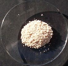
| Appearance | off-white powder |
| Density | 9.68 g/cm3, solid |
| Melting point | 2,758 °C (4,996 °F; 3,031 K) |
| Boiling point | 5,400 °C (9,750 °F; 5,670 K) |
| insoluble | |
| −23.0·10−6 cm3/mol | |
| Hazards | |
| Flash point | Non-flammable |
| Related compounds | |
Other cations
|
Titanium(IV) oxide Zirconium(IV) oxide |
Related compounds
|
Hafnium nitride |
Except where otherwise noted, data are given for materials in their standard state (at 25 °C [77 °F], 100 kPa).
Infobox references
| |
Hafnium(IV) oxide is quite inert. It reacts with strong acids such as concentrated sulfuric acid and with strong bases. It dissolves slowly in hydrofluoric acid to give fluorohafnate anions. At elevated temperatures, it reacts with chlorine in the presence of graphite or carbon tetrachloride to give hafnium tetrachloride.
Structure edit
Hafnia typically adopts the same structure as zirconia (ZrO2). Unlike TiO2, which features six-coordinate Ti in all phases, zirconia and hafnia consist of seven-coordinate metal centres. A variety of other crystalline phases have been experimentally observed, including cubic fluorite (Fm3m), tetragonal (P42/nmc), monoclinic (P21/c) and orthorhombic (Pbca and Pnma).[2] It is also known that hafnia may adopt two other orthorhombic metastable phases (space group Pca21 and Pmn21) over a wide range of pressures and temperatures,[3] presumably being the sources of the ferroelectricity observed in thin films of hafnia.[4]
Thin films of hafnium oxides deposited by atomic layer deposition are usually crystalline. Because semiconductor devices benefit from having amorphous films present, researchers have alloyed hafnium oxide with aluminum or silicon (forming hafnium silicates), which have a higher crystallization temperature than hafnium oxide.[5]
Applications edit
Hafnia is used in optical coatings, and as a high-κ dielectric in DRAM capacitors and in advanced metal–oxide–semiconductor devices.[6] Hafnium-based oxides were introduced by Intel in 2007 as a replacement for silicon oxide as a gate insulator in field-effect transistors.[7] The advantage for transistors is its high dielectric constant: the dielectric constant of HfO2 is 4–6 times higher than that of SiO2.[8] The dielectric constant and other properties depend on the deposition method, composition and microstructure of the material.
Hafnium oxide (as well as doped and oxygen-deficient hafnium oxide) attracts additional interest as a possible candidate for resistive-switching memories[9] and CMOS-compatible ferroelectric field effect transistors (FeFET memory) and memory chips.[10][11][12][13]
Because of its very high melting point, hafnia is also used as a refractory material in the insulation of such devices as thermocouples, where it can operate at temperatures up to 2500 °C.[14]
Multilayered films of hafnium dioxide, silica, and other materials have been developed for use in passive cooling of buildings. The films reflect sunlight and radiate heat at wavelengths that pass through Earth's atmosphere, and can have temperatures several degrees cooler than surrounding materials under the same conditions.[15]
References edit
- ^ Bersch, Eric; et al. (2008). "Band offsets of ultrathin high-k oxide films with Si". Phys. Rev. B. 78 (8): 085114. Bibcode:2008PhRvB..78h5114B. doi:10.1103/PhysRevB.78.085114.
- ^ Table III, V. Miikkulainen; et al. (2013). "Crystallinity of inorganic films grown by atomic layer deposition: Overview and general trends". Journal of Applied Physics. 113 (2): 021301–021301–101. Bibcode:2013JAP...113b1301M. doi:10.1063/1.4757907.
- ^ T. D. Huan; V. Sharma; G. A. Rossetti, Jr.; R. Ramprasad (2014). "Pathways towards ferroelectricity in hafnia". Physical Review B. 90 (6): 064111. arXiv:1407.1008. Bibcode:2014PhRvB..90f4111H. doi:10.1103/PhysRevB.90.064111. S2CID 53347579.
- ^ T. S. Boscke (2011). "Ferroelectricity in hafnium oxide thin films". Applied Physics Letters. 99 (10): 102903. Bibcode:2011ApPhL..99j2903B. doi:10.1063/1.3634052.
- ^ J.H. Choi; et al. (2011). "Development of hafnium based high-k materials—A review". Materials Science and Engineering: R. 72 (6): 97–136. doi:10.1016/j.mser.2010.12.001.
- ^ H. Zhu; C. Tang; L. R. C. Fonseca; R. Ramprasad (2012). "Recent progress in ab initio simulations of hafnia-based gate stacks". Journal of Materials Science. 47 (21): 7399–7416. Bibcode:2012JMatS..47.7399Z. doi:10.1007/s10853-012-6568-y. S2CID 7806254.
- ^ Intel (11 November 2007). "Intel's Fundamental Advance in Transistor Design Extends Moore's Law, Computing Performance".
- ^ Wilk G. D., Wallace R. M., Anthony J. M. (2001). "High-κ gate dielectrics: Current status and materials properties considerations". Journal of Applied Physics. 89 (10): 5243–5275. Bibcode:2001JAP....89.5243W. doi:10.1063/1.1361065.
{{cite journal}}: CS1 maint: multiple names: authors list (link), Table 1 - ^ K.-L. Lin; et al. (2011). "Electrode dependence of filament formation in HfO2 resistive-switching memory". Journal of Applied Physics. 109 (8): 084104–084104–7. Bibcode:2011JAP...109h4104L. doi:10.1063/1.3567915.
- ^ Imec (7 June 2017). "Imec demonstrates breakthrough in CMOS-compatible Ferroelectric Memory".
- ^ The Ferroelectric Memory Company (8 June 2017). "World's first FeFET-based 3D NAND demonstration".
- ^ T. S. Böscke; J. Müller; D. Bräuhaus (7 Dec 2011). "Ferroelectricity in hafnium oxide: CMOS compatible ferroelectric field effect transistors". 2011 International Electron Devices Meeting. IEEE. pp. 24.5.1–24.5.4. doi:10.1109/IEDM.2011.6131606. ISBN 978-1-4577-0505-2.
- ^ Nivole Ahner (August 2018). Mit HFO2 voll CMOS-kompatibel (in German). Elektronik Industrie.
- ^ Very High Temperature Exotic Thermocouple Probes product data, Omega Engineering, Inc., retrieved 2008-12-03
- ^ "Aaswath Raman | Innovators Under 35 | MIT Technology Review". August 2015. Retrieved 2015-09-02.


