


Summary
High-temperature operating life (HTOL) is a reliability test applied to integrated circuits (ICs) to determine their intrinsic reliability. This test stresses the IC at an elevated temperature, high voltage and dynamic operation for a predefined period of time. The IC is usually monitored under stress and tested at intermediate intervals. This reliability stress test is sometimes referred to as a lifetime test, device life test or extended burn in test and is used to trigger potential failure modes and assess IC lifetime.
There are several types of HTOL:
| HTOL Types | Schematic | Description |
|---|---|---|
| Static |  |
IC stressed at static and constant conditions, IC not toggling. |
| Dynamic |  |
Input stimulus for toggling the internal nodes of the device. |
| Monitored | 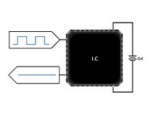 |
Input stimulus for toggling the internal nodes of the device. Live output indicates IC performance. |
| In-situ tested | 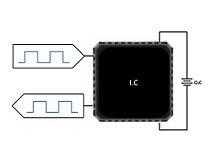 |
Input stimulus for toggling the internal nodes of the device. Responsive output tests IC performance. |
Design considerations edit
The main aim of the HTOL is to age the device such that a short experiment will allow the lifetime of the IC to be predicted (e.g. 1,000 HTOL hours shall predict a minimum of "X" years of operation). Good HTOL process shall avoid relaxed HTOL operation and also prevents overstressing the IC. This method ages all IC's building blocks to allow relevant failure modes to be triggered and implemented in a short reliability experiment. A precise multiplier, known as the Acceleration Factor (AF) simulates long lifetime operation.
The AF represents the accelerated aging factor relative to the useful life application conditions.
For effective HTOL stress testing, several variables should be considered:
- Digital toggling factor
- Analog modules operation
- I/O ring activity
- Monitor design
- Ambient temperature (Ta)
- Junction temperature (Tj)
- Voltage stress (Vstrs)
- Acceleration factor (AF)
- Test duration (t)
- Sample size (SS)
A detailed description of the above variables, using a hypothetical, simplified IC with several RAMs, digital logic, an analog voltage regulator module and I/O ring, together with the HTOL design considerations for each are provided below.
Digital toggling factor edit
The digital toggling factor (DTF) represents the number of transistors that change their state during the stress test, relative to the total number of gates in the digital portion of the IC. In effect, the DTF is the percentage of transistors toggling in one time unit. The time unit is relative to the toggling frequency, and is usually limited by the HTOL setup to be in the range of 10–20Mhz.
Reliability engineers strive to toggle as many as possible transistors for each time unit of measure. The RAMs (and other memory types) are usually activated using the BIST function, while the logic is usually activated with the SCAN function, LFSR or logic BIST.
The power and the self-heating of the digital portion of the IC are evaluated and the device's aging estimated. These two measures are aligned so that they are similar to the aging of other elements of the IC. The degrees of freedom for aligning these measures are the voltage stress and/or the time period during which the HTOL program loops these blocks relative to other IC blocks.
Analog modules operation edit
The recent trend of integrating as many electronic components as possible into a single chip is known as system on a chip (SoC).
This trend complicates reliability engineers' work because (usually) the analog portion of the chip dissipates higher power relative to the other IC elements.
This higher power may generate hot spots and areas of accelerated aging. Reliability engineers must understand the power distribution on the chip and align the aging so that it is similar for all elements of an IC.
In our hypothetical SoC the analog module only includes a voltage regulator. In reality, there may be additional analog modules e.g. PMIC, oscillators, or charge pumps. To perform efficient stress tests on the analog elements, reliability engineers must identify the worst-case scenario for the relevant analog blocks in the IC. For example, the worst-case scenario for voltage regulators may be the maximum regulation voltage and maximum load current; for charge pumps it may be the minimum supply voltage and maximum load current.
Good engineering practice calls for the use of external loads (external R,L,C) to force the necessary currents. This practice avoids loading differences due to the chip's different operational schemes and operation trimming of its analog parts.
Statistical methods are used to check statistical tolerances, variation and temperature stability of the loads used, and to define the right confidence bands for the loads to avoid over/under stress at HTOL operating range. The degrees of freedom for aligning the aging magnitude of analog parts is usually the duty-cycle, external load values and voltage stress.
I/O ring activity edit
The interface between the "outside world" and the IC is made via the input/output (I/O) ring. This ring contains power I/O ports, digital I/O ports and analog I/O ports. The I/Os are (usually) wired via the IC package to the "outside world" and each I/O executes its own specific command instructions, e.g. JTAG ports, IC power supply ports etc. Reliability engineering aims to age all I/Os in the same way as the other IC elements. This can be achieved by using a Boundary scan operation.
Monitor design edit
As previously mentioned, the main aim of the HTOL is aging the samples by dynamic stress at elevated voltage and/or temperature. During the HTOL operation, we need to assure that the IC is active, toggling and constantly functioning.
At the same time, we need to know at what point the IC stops responding, these data are important for calculating price reliability indices and for facilitating the FA. This is done by monitoring the device via one or more vital IC parameters signals communicated and logged by the HTOL machine and providing continuous indication about the IC's functionality throughout the HTOL run time. Examples of commonly used monitors include the BIST "done" flag signal, the SCAN output chain or the analog module output.
There are three types of monitoring:
- Pattern matching: The actual output signal is compared to the expected one and alerts about any deviation. The main disadvantage of this monitor type is its sensitivity to any minor deviation from the expected signal. During the HTOL, the IC runs at a temperature and/or voltages that occasionally fall outside its specification, which may cause artificial sensitivity and/or a malfunction that fails the matching but is not a real failure.
- Activity: Counts the number of toggles and if the results are higher than a predefined threshold the monitor indicates OK. The main disadvantage of this type of monitoring is the chance that unexpected noise or signal could be wrongly interpreted. This issue arises mainly in the case of low count toggling monitor.
- Activity within a predefine range: Checks that the monitor responds within a predefined limit, for example when then number of toggles is within a predefined limit or the output of the voltage regulator is within a predefined range.
Ambient temperature (Ta) edit
According to JEDEC standards, the environmental chamber should be capable of maintaining the specified temperature within a tolerance of ±5 °C throughout while parts are loaded and unpowered. Today's environmental chambers have better capabilities and can exhibit temperature stability within a range of ±3 °C throughout.
Junction temperature (Tj) edit
Low power ICs can be stressed without major attention to self-heating effects. However, due to technology scaling and manufacturing variations, power dissipation within a single production lot of devices can vary by as much as 40%. This variation, in addition to high power IC makes advanced contact temperature controls necessary for facilitating individual control systems for each IC
Voltage stress (Vstrs) edit
The operating voltage should be at least the maximum specified for the device. In some cases a higher voltage is applied to obtain lifetime acceleration from voltage as well as temperature.
To define the maximum permitted voltage stress, the following methods can be considered:
- Force 80% of breakdown voltage;
- Force six-sigma less than the breakdown voltage;
- Set the overvoltage to be higher than the maximum specified voltage. An overvoltage level of 140% of the maximum voltage is occasionally used for MIL and automotive applications.
Reliability engineers must check that Vstress does not exceed the maximum rated voltage for the relevant technology, as specified by the FAB.
Acceleration factor (AF) edit
The Acceleration factor (AF) is a multiplier that relates a product's life at an accelerated stress level to the life at the use stress level.
An AF of 20 means 1 hour at stress condition is equivalent to 20 hours at useful condition.
The voltage acceleration factor is represented by AFv. Usually the stress voltage is equal to or higher than the maximum voltage. An elevated voltage provides additional acceleration and can be used to increase effective device hours or achieve an equivalent life point.
There are several AFv models:
- E model or the constant field/voltage acceleration exponential model;
- 1/E model or, equivalently, the anode hole injection model;
- V model, where the failure rate is exponential to voltage
- Anode hydrogen release for the power-law model
AFtemp is the acceleration factor due to changes in temperature and is usually based on the Arrhenius equation. The total acceleration factor is the product of AFv and AFtemp
Test duration (t) edit
The reliability test duration assures the device's adequate lifetime requirement.
For example, with an activation energy of 0.7 eV, 125 °C stress temperature and 55 °C use temperature, the acceleration factor (Arrhenius equation) is 78.6. This means that 1,000 hours' stress duration is equivalent to 9 years of use. The reliability engineer decides on the qualification test duration. Industry good practice calls for 1,000 hours at a junction temperature of 125 °C.
Sample size (SS) edit
The challenge for new reliability assessment and qualification systems is determining the relevant failure mechanisms to optimize sample size.
Sample plans are statistically derived from manufacturer risk, consumer risk, and the expected failure rate. The commonly used sampling plan of zero rejects out of 230 samples is equal to three rejects out of 668 samples assuming LTPD =1 and a 90% confidence interval.
HTOL policy edit
Sample selection edit
Samples shall include representative samples from at least three nonconsecutive lots to represent manufacturing variability. All test samples shall be fabricated, handled, screened and assembled in the same way as during the production phase.
Sample preparation edit
Samples shall be tested prior to stress and at predefined checkpoints. It is good engineering practice to test samples at maximum and minimum rating temperatures as well as at room temperature. Data logs of all functional and parametric tests shall be collated for further analysis.
Test duration edit
Assuming Tj = 125 °C, commonly used checkpoints are after 48, 168, 500 and 1,000 hours.
Different checkpoints for different temperatures can be calculated by using the Arrhenius equation. For example, with an activation energy of 0.7e V, Tj of 135 °C and Tuse of 55 °C the equivalent checkpoints will be at 29, 102, 303 and 606 hours.
Electrical testing should be completed as soon as possible after the samples are removed. If the samples cannot be tested soon after their removal, additional stress time should be applied. The JEDEC standard requires samples be tested within 168 hours of removal.
If testing exceeds the recommended time window, additional stress should be applied according to the table below:[2]
| Time above recommended time window | 0h < h ≤ 168h | 168h < h ≤ 336h | 336h < h ≤ 504h | Other |
|---|---|---|---|---|
| Additional stress hours | 24h | 48h | 72h | 24 hours for each 168 hours |
Merit numbers edit
The merit number is the outcome of statistical sampling plans.
Sampling plans are inputted to SENTENCE, an audit tool, to ensure that the output of a process meets the requirements. SENTENCE simply accepts or rejects the tested lots. The reliability engineer implements statistical sampling plans based on predefined Acceptance Quality Limits, LTPD, manufacturer risk and customer risk. For example, the commonly used sampling plan of 0 rejects out of 230 samples is equal to 3 rejects out of 668 samples assuming LTPD=1.
HTOL in various industries edit
The aging process of an IC is relative to its standard use conditions. The tables below provide reference to various commonly used products and the conditions under which they are used.
Reliability engineers are tasked with verifying the adequate stress duration. For example, for an activation energy of 0.7eV, a stress temperature of 125 °C and a use temperature of 55 °C, an expected operational life of five years is represented by a 557-hour HTOL experiment.
Commercial use edit
| Min Tuse | Max Tuse | Description | Expected life time |
|---|---|---|---|
| 5 °C | 50 °C | desktop products | 5 years |
| 0 °C | 70 °C | mobile products | 4 years |
Automotive use edit
Example Automotive Use Conditions[1]
| Min Tuse | Max Tuse | Description | Expected life time |
|---|---|---|---|
| −40 °C | 105—150 °C | under hood condition | 10 to 15 years |
| −40 °C | 80 °C | passenger compartment condition | 10 to 15 years |
| 0 °C | 70 °C | passenger compartment condition | 10 to 15 years |
Telecommunication use edit
Example European Telecom use Conditions definition
| Min Tuse | Max Tuse | Description | Expected life time |
|---|---|---|---|
| 5 °C | 40 °C | class 3.1 Temperature-controlled locations | usually 25 years |
| −5 °C | 45 °C | class 3.2 Partly temperature-controlled locations | usually 25 years |
| −25 °C | 55 °C | class 3.3 Not temperature-controlled locations | usually 25 years |
| −40 °C | 70 °C | class 3.4 Sites with heat-trap | usually 25 years |
| −40 °C | 40 °C | class 3.5 Sheltered locations, Direct solar radiation | usually 25 years |
Example US Telecom use conditions definition
| Min Tuse | Max Tuse | Description | Expected life time |
|---|---|---|---|
| −40 °C | 46 °C | Uncontrolled environment | 25 years |
| 5 °C | 40 °C | Enclosed building | 25 years |
Military use edit
Example military use conditions
| Min Tuse | Max Tuse | Description |
|---|---|---|
| −55 °C | 125 °C | MIL products |
| −55 °C | up to 225 °C | high-temp applications |
Example edit
Number of Failures = r
Number of Devices = D
Test Hours per Device = H
Celsius + 273 = T (Calculation Temperature in Kelvin)
Test Temperature (HTRB or other burn-in temperature)=

Use Temperature (standardized at 55 °C or 328K) =

Activation Energy (eV) =

Chi Squared/2 is the probability estimation for number of failures at α and ν

- Confidence Level for X^2 distribution; reliability calculations use α=60% or .60 = α (alpha)
- Degrees of Freedom for distribution; reliability calculations use ν=2r + 2. = ν (nu)

Acceleration Factor from the Arrhenius equation =

Boltzmann's Constant ( ) = 8.617 x 10e-5 eV/K

Device Hours (DH) = D x H
Equivalent Device Hours (EDH) = D x H x
Failure Rate per hour =

Failures in Time = Failure Rate per billion hours = FIT =

Mean Time to Failure = MTTF
Where the Acceleration Factor from the Arrhenius equation is:

Failure Rate per hour =

Failures in Time = Failure Rate per billion hours = FIT =

Mean Time to Failure in hours =

Mean Time to Failure in years= ´

In case you want to calculate the acceleration factor including the Humidity the so-called Highly accelerated stress test (HAST), then:
the Acceleration Factor from the Arrhenius equation would be:

where is the stress test relative humidity (in percentage). Typically is 85%.

where is the typical use relative humidity (in percentage). Typically this is measured at the chip surface ca. 10–20%.

where is the failure mechanism scale factor. Which is a value between 0.1 and 0.15.

In case you want to calculate the acceleration factor including the Humidity (HAST) and voltage stress then:
the Acceleration Factor from the Arrhenius equation would be:

where is the stress voltage (in volts). Typically is the VCCx1.4 volts. e.g. 1.8x1.4=2.52 volts.

where is the typical usage voltage or VCC (in volts). Typically VCC is 1.8v. Depending on the design.

where is the failure mechanism scale factor. Which is a value between 0 and 3.0. Typically 0.5 for Silican junction defect.

See also edit
References edit
External links edit
- siliconfareast
- Comparing the Effectiveness of Stress-based Reliability Qualification Stress Conditions
- Reliability Hotwire eMagazine
- SEMATECH Handbook