


Summary
Indium(II) selenide (InSe) is an inorganic compound composed of indium and selenium. It is a III-VI layered semiconductor. The solid has a structure consisting of two-dimensional layers bonded together only by van der Waals forces. Each layer has the atoms in the order Se-In-In-Se.[2]
| Identifiers | |
|---|---|
| |
3D model (JSmol)
|
|
| ChemSpider |
|
PubChem CID
|
|
| |
| |
| Properties | |
| InSe | |
| Molar mass | 193.789 g·mol−1 |
| Density | 5.0 |
| Melting point | 611 °C (1,132 °F; 884 K)[1] |
Except where otherwise noted, data are given for materials in their standard state (at 25 °C [77 °F], 100 kPa).
Infobox references
| |
Potential applications are for field effect transistors, optoelectronics, photovoltaic, non-linear optics, strain gauges,[2] and methanol gas sensors.[3]
Formation edit
Indium(II) selenide can be formed via a number of different methods. A method to make the bulk solid is the Bridgman/Stockbarger method, in which the elements indium and selenium are heated to over 900 °C in a sealed capsule, and then slowly cooled over about a month.[4] Another method is electrodeposition from a water solution of indium(I) sulfate and selenium dioxide.[5]
Properties edit
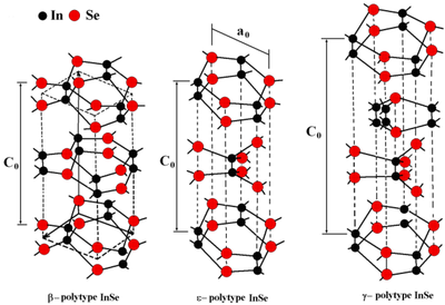
There are three polytopes or crystal forms. β, ε are hexagonal with unit cells spanning two layers. γ has rhombohedral crystal system, with the unit cell including four layers.[2]
β-Indium(II) selenide can be exfoliated into two-dimensional sheets using sticky tape. In a vacuum these form smooth layers. However when exposed to air, the layers become corrugated because of chemisorption of air molecules.[6] Exfoliation can also take place in isopropanol liquid.[7]
Indium (II) selenide is stable in ambient conditions of oxygen and water vapour, unlike many other semiconductors.[2]
| polytope | space group | unit cell | band gap | eV |
|---|---|---|---|---|
| β | P63/mmc | a=4.005 c=16.660 Z=4 | direct | 1.28 |
| γ | R3m | a=7.1286 Å, c=19.382 Å and Z=6 | direct | 1.29 |
| ε | P6m2 | indirect | 1.4 |
Doping edit
The properties of indium(II) selenide can be varied by way of altering the exact ratio of elements from 1:1, creating vacancies. It is hard to get an exact equality. The properties can be compensated by transition element doping. Other elements that can be included in small concentrations are boron,[8] silver,[9] and cadmium.[10]
References edit
- ^ Teena, M.; Kunjomana, A. G. (April 2018). "Crystal shape engineering and studies on the performance of vapour deposited InSe platelets". Journal of Materials Science: Materials in Electronics. 29 (7): 5536–5547. doi:10.1007/s10854-018-8522-5. S2CID 103682866.
- ^ a b c d Politano, A.; Campi, D.; Cattelan, M.; Ben Amara, I.; Jaziri, S.; Mazzotti, A.; Barinov, A.; Gürbulak, B.; Duman, S.; Agnoli, S.; Caputi, L. S.; Granozzi, G.; Cupolillo, A. (December 2017). "Indium selenide: an insight into electronic band structure and surface excitations". Scientific Reports. 7 (1): 3445. Bibcode:2017NatSR...7.3445P. doi:10.1038/s41598-017-03186-x. PMC 5469805. PMID 28611385.

- ^ Marvan, Petr; Mazánek, Vlastimil; Sofer, Zdeněk (2019). "Shear-force exfoliation of indium and gallium chalcogenides for selective gas sensing applications". Nanoscale. 11 (10): 4310–4317. doi:10.1039/C8NR09294J. PMID 30788468. S2CID 206138673.
- ^ a b Boukhvalov, Danil; Gürbulak, Bekir; Duman, Songül; Wang, Lin; Politano, Antonio; Caputi, Lorenzo; Chiarello, Gennaro; Cupolillo, Anna (5 November 2017). "The Advent of Indium Selenide: Synthesis, Electronic Properties, Ambient Stability and Applications". Nanomaterials. 7 (11): 372. doi:10.3390/nano7110372. PMC 5707589. PMID 29113090.
- ^ Demir, Kübra Çınar; Demir, Emre; Yüksel, Seniye; Coşkun, Cevdet (December 2019). "Influence of deposition conditions on nanostructured InSe thin films". Current Applied Physics. 19 (12): 1404–1413. Bibcode:2019CAP....19.1404D. doi:10.1016/j.cap.2019.09.008. S2CID 203143299.
- ^ Dmitriev, A. I.; Vishnjak, V. V.; Lashkarev, G. V.; Karbovskyi, V. L.; Kovaljuk, Z. D.; Bahtinov, A. P. (March 2011). "Investigation of the morphology of the van der Waals surface of the InSe single crystal". Physics of the Solid State. 53 (3): 622–633. Bibcode:2011PhSS...53..622D. doi:10.1134/S1063783411030085. S2CID 121113583.
- ^ Petroni, Elisa; Lago, Emanuele; Bellani, Sebastiano; Boukhvalov, Danil W.; Politano, Antonio; Gürbulak, Bekir; Duman, Songül; Prato, Mirko; Gentiluomo, Silvia; Oropesa-Nuñez, Reinier; Panda, Jaya-Kumar; Toth, Peter S.; Del Rio Castillo, Antonio Esau; Pellegrini, Vittorio; Bonaccorso, Francesco (June 2018). "Liquid-Phase Exfoliated Indium-Selenide Flakes and Their Application in Hydrogen Evolution Reaction". Small. 14 (26): 1800749. arXiv:1903.08967. doi:10.1002/smll.201800749. PMID 29845748. S2CID 44172633.
- ^ Ertap, Hüseyin; Karabulut, Mevlut (5 December 2018). "Structural and electrical properties of boron doped InSe single crystals". Materials Research Express. 6 (3): 035901. doi:10.1088/2053-1591/aaf2f6. S2CID 105206868.
- ^ Gürbulak, Bekir; Şata, Mehmet; Dogan, Seydi; Duman, Songul; Ashkhasi, Afsoun; Keskenler, E. Fahri (November 2014). "Structural characterizations and optical properties of InSe and InSe:Ag semiconductors grown by Bridgman/Stockbarger technique". Physica E: Low-dimensional Systems and Nanostructures. 64: 106–111. Bibcode:2014PhyE...64..106G. doi:10.1016/j.physe.2014.07.002.
- ^ Evtodiev, Igor (2009). "Excitonic absorption of the light in heterojunctions Bi 2 O 3-InSe".