


Summary
Low-temperature polycrystalline silicon (LTPS) is polycrystalline silicon that has been synthesized at relatively low temperatures (~650 °C and lower) compared to in traditional methods (above 900 °C). LTPS is important for display industries, since the use of large glass panels prohibits exposure to deformative high temperatures. More specifically, the use of polycrystalline silicon in thin-film transistors (LTPS-TFT) has high potential for large-scale production of electronic devices like flat panel LCD displays or image sensors.[1]
Development of polycrystalline silicon edit
Polycrystalline silicon (p-Si) is a pure and conductive form of the element composed of many crystallites, or grains of highly ordered crystal lattice. In 1984, studies showed that amorphous silicon (a-Si) is an excellent precursor for forming p-Si films with stable structures and low surface roughness.[2] Silicon film is synthesized by low-pressure chemical vapor deposition (LPCVD) to minimize surface roughness. First, amorphous silicon is deposited at 560–640 °C. Then it is thermally annealed (recrystallized) at 950–1000 °C. Starting with the amorphous film, rather than directly depositing crystals, produces a product with a superior structure and a desired smoothness.[3][4] In 1988, researchers discovered that further lowering temperature during annealing, together with advanced plasma-enhanced chemical vapor deposition (PECVD), could facilitate even higher degrees of conductivity. These techniques have profoundly impacted the microelectronics, photovoltaic, and display enhancement industries.
Use in liquid-crystal display edit

Amorphous silicon TFTs have been widely used in liquid-crystal display (LCD) flat panels because they can be assembled into complex high-current driver circuits. Amorphous Si-TFT electrodes drive the alignment of crystals in LCDs. The evolution to LTPS-TFTs can have many benefits such as higher device resolution, lower synthesis temperature, and reduced price of essential substrates.[5] However, LTPS-TFTs also have several drawbacks. For example, the area of TFTs in traditional a-Si devices is large, resulting in a small aperture ratio (the amount of area which is not blocked by the opaque TFT and thus admits light). The incompatibility of different aperture ratios prevents LTPS-based complex circuits and drivers from being integrated into a-Si material.[6] Additionally, the quality of LTPS decreases over time due to an increase in temperature upon turning on the transistor, which degrades the film by breaking the Si-H bonds in the material. This would cause the device to suffer from drain breakdown and current leakage,[7] most notably in small and thin transistors, which dissipate heat poorly.[8]
Processing by laser annealing edit

XeCl Excimer-Laser Annealing (ELA) is the first key method to produce p-Si by melting a-Si material through laser irradiation. The counterpart of a-Si, polycrystalline silicon, which can be synthesized from amorphous silicon by certain procedures, has several advantages over widely used a-Si TFT:
- High electron mobility rate;
- High resolution and aperture ratio;
- Available for high integration of circuits.[9]
XeCl-ELA succeeds in crystallizing a-Si (thickness ranges from 500-10000Å) into p-Si without heating the substrates.[10] The polycrystalline form has larger grains that yield better mobility for TFTs due to reduced scattering from grain boundaries.[11][12][13] This technique leads to the successful integration of complicated circuits in LCD displays.[14]
Development of LTPS-TFT devices edit
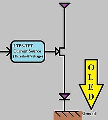
Apart from the improvement of the TFTs themselves, the successful application of LTPS to graphic display also depends on innovative circuits. One recent technique involves a pixel circuit in which the outgoing current from the transistor is independent of the threshold voltage, thus producing uniform brightness.[15][16] LTPS-TFT is commonly used to drive organic light-emitting diode (OLED) displays because it has high resolution and accommodation for large panels. However, variations in LTPS structure would result in non-uniform threshold voltage for signals and non-uniform brightness using traditional circuits. The new pixel circuit includes four n-type TFTs, one p-type TFT, a capacitor, and a control element to control the image resolution.[16] Enhancing the performance and microlithography for TFTs is important for advancing LTPS active-matrix OLEDs. These many important techniques have allowed the mobility of crystalline film to reach up to 13 cm2/Vs, and they have helped to mass-produce LEDs and LCDs over 500 ppi in resolution.[10]
| Characteristic | Amorphous Si | Polycrystalline Si |
|---|---|---|
| Mobility (cm^2 /(V*s)) | 0.5 | >500 |
| Deposition Method | PECVD | ELA |
| Deposition Temperature | 350 °C | 600 °C |
| Driver Integration | Only partial | System-on-glass |
| Resolution | Low | >500 ppi |
| Cost | Low | Relatively higher |
LTPO edit
Low-temperature polycrystalline oxide (LTPO) is a type of OLED display backplane technology developed by Apple that combines both LTPS TFTs and oxide TFTs (indium gallium zinc oxide, or IGZO). In LTPO, the switching circuits are using LTPS while the driving TFTs use IGZO materials.[17] LTPO allows for more efficient use of power by dynamically adjusting the refresh rate of the screen based on the content being displayed. This means that the screen can operate at a low refresh rate when displaying static images or text, but can ramp up to a higher refresh rate when displaying dynamic content like videos or games. LTPO displays are known for their improved battery life and can be found in some smartphones, smartwatches, and other mobile devices.[18]
Although the core technology in LTPO is developed by Apple, Samsung also has its proprietary technology for LTPO AMOLED panels using a combination of LTPS TFTs and hybrid-oxide and polycrystalline silicon (HOP).[19]
See also edit
References edit
- ^ Fonash, Stephen. "Low Temperature Crystallization and Patterning of Amorphous Silicon Film On Electrically Insulating Substrates." United States Patent (1994). Print.
- ^ Harbeke, G., L. Krausbauer, E.F. Steigmerier, and A.E. Widmer. "Growth and Physical Properties of LPCVD Polycrystalline Silicon Films." Journal of the Electrochemical Society (1984): 675. Print.
- ^ Hatalis, Miltiadis K., and David W. Greve. "Large Grain Polycrystalline Silicon By Low-Temperature Annealing Of Low-Pressure Chemical Vapor Deposited Amorphous Silicon Films." Applied Physics 63.07 (1988): 2266. Print.
- ^ Hatalis, M.K., and D.W. Greve. "High-Performance Thin-Film Transistors In Low-Temperature Crystallized LPCVD Amorphous Silicon Films." IEEE Electron Device Letters 08 (1987): 361–64. Print.
- ^ Zhiguo, Meng, Mingxiang Wang, and Man Wong. "High Performance Low Temperature Metal-Induced Unilaterally Crystallized Polycrystalline Silicon Thin Film Transistors for System-on-Panel Application." IEEE Transactions On Electron Devices 47.02 (2000). Print.
- ^ Inoue, Satoshi, Hiroyuki Ohshima, and Tatsuya Shimoda. "Analysis of Degradation Phenomenon Caused by Self-Heating in Low-Temperature-Processed Polycrystalline Silicon Thin Film Transistors." Japanese Journal of Applied Physics 41 (2002): 6313-319. IOP Sciences. Web. 2 Mar. 2015.
- ^ Lui, Basil; Quinn, M.J.; Tam, S.W.-B.; Brown, T.M.; Migliorato, P.; Ohshima, H. (1998). "Investigation of the low field leakage current mechanism in polysilicon TFT's". IEEE Transactions on Electron Devices. 45 (1): 213–217. doi:10.1109/16.658833. ISSN 1557-9646.
- ^ G. A. Bhat, Z. Jin, H. S. Kwok, and M. Wong, “Effect of MIC/MILC Interface On The Performance Of MILC-TFT’s,” in Dig. 56th Annu. Device Research Conf., June 22–24, 1998, pp. 110–111.
- ^ Kuo, Yue. "Thin Film Transistor Technology—Past, Present, and Future." The Electrochemical Society Interface (2013). Electrochemical Society Interface. Web. 1 Mar. 2015.
- ^ a b Sameshima, T., S. Usui, and M. Sekiya. "XeClExcimer Laser Annealing Used in the Fabrication of Poly-Si TFT's." IEEE Electron Device Letters 07.05 (1986): 276-78. IEEE Xplore. Web. 2 Mar. 2015.
- ^ Kimura, Mutsumi; Inoue, Satoshi; Shimoda, Tatsuya; Tam, Simon W.-B.; Lui, Basil; Migliorato, Piero; Nozawa, Ryoichi (2002-03-15). "Extraction of trap states in laser-crystallized polycrystalline-silicon thin-film transistors and analysis of degradation by self-heating". Journal of Applied Physics. 91 (6): 3855–3858. doi:10.1063/1.1446238. ISSN 0021-8979.
- ^ Lui, Basil; Tam, S. W.-B.; Migliorato, P.; Shimoda, T. (2001-06-01). "Method for the determination of bulk and interface density of states in thin-film transistors". Journal of Applied Physics. 89 (11): 6453–6458. doi:10.1063/1.1361244. ISSN 0021-8979.
- ^ Kimura, Mutsumi; Inoue, Satoshi; Shimoda, Tatsuya; Lui, Basil; French, William; Kamohara, Itaru; Migliorato, Piero (2001). "Development of poly-Si TFT models for device simulation: In-plane trap model and thermionic emission model". SID Conference Record of the International Display Research Conference (in Japanese): 423–426. ISSN 1083-1312.
- ^ Uchikoga, Shuichi. "Low-Temperature Polycrystalline Silicon Thin-Film Transistor Technologies for System-on-Glass Displays." MRS Bulletin (2002): 881-86. Google Scholar. MRS Bulletin. Web. 2 Mar. 2015.
- ^ Banger, K. K., Y. Yamashita, K. Mori, R. L. Peterson, T. Leedham, J. Rickard, and H. Sirringhaus. "Low-temperature, High-performance Solution-processed Metal Oxide Thin-film Transistors Formed by a ‘sol–gel on Chip’ Process." Nature Materials (2010): 45–50. Nature Materials. Web. 2 Mar. 2015.
- ^ a b Tai, Y.-H., B.-T. Chen, Y.-J. Kuo, C.-C. Tsai, K.-Y. Chiang, Y.-J. Wei, and H.-C. Cheng. "A New Pixel Circuit for Driving Organic Light-Emitting Diode With Low Temperature Polycrystalline Silicon Thin-Film Transistors." Journal of Display Technology 01.01 (2015): 100-104. IEEE Xplore. Web. 2 Mar. 2015.
- ^ Mertens, Ron (2019-02-10). "LTPO backplane technology - introduction and news". OLED Info. Retrieved 2023-02-24.
- ^ Moore-Colyer, Roland (2021-04-02). "What is LTPO? How this tech delivers killer phone displays". Tom's Guide. Retrieved 2023-02-24.
- ^ "Samsung Display's LTPO tech is called HOP". THE ELEC, Korea Electronics Industry Media. 2020-06-16. Retrieved 2023-02-24.