


Summary
In crystallography, a stacking fault is a planar defect that can occur in crystalline materials.[1][2] Crystalline materials form repeating patterns of layers of atoms. Errors can occur in the sequence of these layers and are known as stacking faults. Stacking faults are in a higher energy state which is quantified by the formation enthalpy per unit area called the stacking-fault energy. Stacking faults can arise during crystal growth or from plastic deformation. In addition, dislocations in low stacking-fault energy materials typically dissociate into an extended dislocation, which is a stacking fault bounded by partial dislocations.
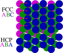

The most common example of stacking faults is found in close-packed crystal structures. Face-centered cubic (fcc) structures differ from hexagonal close packed (hcp) structures only in stacking order: both structures have close-packed atomic planes with sixfold symmetry — the atoms form equilateral triangles. When stacking one of these layers on top of another, the atoms are not directly on top of one another. The first two layers are identical for hcp and fcc, and labelled AB. If the third layer is placed so that its atoms are directly above those of the first layer, the stacking will be ABA — this is the hcp structure, and it continues ABABABAB. However, there is another possible location for the third layer, such that its atoms are not above the first layer. Instead, it is the atoms in the fourth layer that are directly above the first layer. This produces the stacking ABCABCABC, which is in the [111] direction of a cubic crystal structure. In this context, a stacking fault is a local deviation from one of the close-packed stacking sequences to the other one. Usually, only one- two- or three-layer interruptions in the stacking sequence are referred to as stacking faults. An example for the fcc structure is the sequence ABCABABCAB.
Formation of stacking faults in FCC crystal edit
Stacking faults are two dimensional planar defects that can occur in crystalline materials. They can be formed during crystal growth, during plastic deformation as partial dislocations move as a result of dissociation of a perfect dislocation, or by condensation of point defects during high-rate plastic deformation.[3] The start and finish of a stacking fault are marked by partial line dislocations such as a partial edge dislocation. Line dislocations tend to occur on the closest packed plane in the closest packed direction. For an FCC crystal, the closest packed plane is the (111) plane, which becomes the glide plane, and the closest packed direction is the [110] direction. Therefore, a perfect line dislocation in FCC has the burgers vector ½<110>, which is a translational vector.[4]
Splitting into two partial dislocations is favorable because the energy of a line defect is proportional to the square of the burger’s vector magnitude. For example, an edge dislocation may split into two Shockley partial dislocations with burger’s vector of 1/6<112>.[4] This direction is no longer in the closest packed direction, and because the two burger’s vectors are at 60 degrees with respect to each other in order to complete a perfect dislocation, the two partial dislocations repel each other. This repulsion is a consequence of stress fields around each partial dislocation affecting the other. The force of repulsion depends on factors such as shear modulus, burger’s vector, Poisson’s ratio, and distance between the dislocations.[4]
As the partial dislocations repel, stacking fault is created in between. By nature of stacking fault being a defect, it has higher energy than that of a perfect crystal, so acts to attract the partial dislocations together again. When this attractive force balance the repulsive force described above, the defects are in equilibrium state.[4]
The stacking fault energy can be determined from the width of dislocation dissociation using[4]

where and are the burgers vectors and is the vector magnitude for the dissociated partial dislocations, is the shear modulus, and the distance between the partial dislocations.


Stacking faults may also be created by Frank partial dislocations with burger’s vector of 1/3<111>.[4] There are two types of stacking faults caused by Frank partial dislocations: intrinsic and extrinsic. An intrinsic stacking fault forms by vacancy agglomeration and there is a missing plane with sequence ABCA_BA_BCA, where BA is the stacking fault.[5] An extrinsic stacking fault is formed from interstitial agglomeration, where there is an extra plane with sequence ABCA_BAC_ABCA.[5]
Visualizing stacking faults using electron microscopy edit
Stacking faults can be visualized using electron microscopy.[6] One commonly used technique is transmission electron microscopy (TEM). The other is electron channeling contrast imaging (ECCI) in scanning electron microscope (SEM).
In an SEM, near-surface defects can be identified because backscattered electron yield differs in defect regions where the crystal is strained, and this gives rise to different contrasts in the image. In order to identify the stacking fault, it is important to recognize the exact Bragg condition for certain lattice planes in the matrix such that regions without defects will detect little backscattered electrons and thus appear dark. Meanwhile, regions with the stacking fault will not satisfy the Bragg condition and thus yield high amounts of backscattered electrons, and thus appear bright in the image. Inverting the contrast gives images where the stacking fault appears dark in the midst of a bright matrix.[7]
In a TEM, bright field imaging is one technique used to identify the location of stacking faults. Typical image of stacking fault is dark with bright fringes near a low-angle grain boundary, sandwiched by dislocations at the end of the stacking fault. Fringes indicate that the stacking fault is at an incline with respect to the viewing plane.[3]
Stacking faults in semiconductors edit
Many compound semiconductors, e.g. those combining elements from groups III and V or from groups II and VI of the periodic table, crystallize in the fcc zincblende or hcp wurtzite crystal structures. In a semiconductor crystal, the fcc and hcp phases of a given material will usually have different band gap energies. As a consequence, when the crystal phase of a stacking fault has a lower band gap than the surrounding phase, it forms a quantum well, which in photoluminescence experiments leads to light emission at lower energies (longer wavelengths) than for the bulk crystal.[8] In the opposite case (higher band gap in the stacking fault), it constitutes an energy barrier in the band structure of the crystal that can affect the current transport in semiconductor devices.
References edit
- ^ Fine, Morris E. (1921). "Introduction to Chemical and Structural Defects in Crystalline Solids", in Treatise on Solid State Chemistry Volume 1, Springer.
- ^ Hirth, J. P. & Lothe, J. (1992). Theory of dislocations (2 ed.). Krieger Pub Co. ISBN 0-89464-617-6.
- ^ a b Li, B.; Yan, P. F.; Sui, M. L.; Ma, E. Transmission Electron Microscopy Study of Stacking Faults and Their Interaction with Pyramidal Dislocations in Deformed Mg. Acta Materialia 2010, 58 (1), 173–179. doi:10.1016/j.actamat.2009.08.066.
- ^ a b c d e f Hull, D.; Bacon, D. Chapter 5. Dislocations in Face-Centered Cubic Metals. In Introduction to Dislocations; 2011; pp 85–107.
- ^ a b 5.4.1 Partial Dislocations and Stacking Faults http://dtrinkle.matse.illinois.edu/MatSE584/kap_5/backbone/r5_4_1.html .
- ^ Spence, J. C. H.; et al. (2006). "Imaging dislocation cores - the way forward". Philos. Mag. 86 (29–31): 4781. Bibcode:2006PMag...86.4781S. doi:10.1080/14786430600776322. S2CID 135976739.
- ^ Weidner, A.; Glage, A.; Sperling, L.; Biermann, H. Observation of Stacking Faults in a Scanning Electron Microscope by Electron Channelling Contrast Imaging. IJMR 2011, 102 (1), 3–5. doi:10.3139/146.110448.
- ^ Lähnemann, J.; Jahn, U.; Brandt, O.; Flissikowski, T.; Dogan, P.; Grahn, H.T. (2014). "Luminescence associated with stacking faults in GaN". J. Phys. D: Appl. Phys. 47 (42): 423001. arXiv:1405.1261. Bibcode:2014JPhD...47P3001L. doi:10.1088/0022-3727/47/42/423001. S2CID 118671207.