


Summary
Surface plasmon polaritons (SPPs) are electromagnetic waves that travel along a metal–dielectric or metal–air interface, practically in the infrared or visible-frequency. The term "surface plasmon polariton" explains that the wave involves both charge motion in the metal ("surface plasmon") and electromagnetic waves in the air or dielectric ("polariton").[1]
They are a type of surface wave, guided along the interface in much the same way that light can be guided by an optical fiber. SPPs have a shorter wavelength than light in vacuum at the same frequency (photons).[2] Hence, SPPs can have a higher momentum and local field intensity.[2] Perpendicular to the interface, they have subwavelength-scale confinement. An SPP will propagate along the interface until its energy is lost either to absorption in the metal or scattering into other directions (such as into free space).
Application of SPPs enables subwavelength optics in microscopy and photolithography beyond the diffraction limit. It also enables the first steady-state micro-mechanical measurement of a fundamental property of light itself: the momentum of a photon in a dielectric medium. Other applications are photonic data storage, light generation, and bio-photonics.[2][3][4][5]
Excitation edit


SPPs can be excited by both electrons and photons. Excitation by electrons is created by firing electrons into the bulk of a metal.[6] As the electrons scatter, energy is transferred into the bulk plasma. The component of the scattering vector parallel to the surface results in the formation of a surface plasmon polariton.[7]
For a photon to excite an SPP, both must have the same frequency and momentum. However, for a given frequency, a free-space photon has less momentum than an SPP because the two have different dispersion relations (see below). This momentum mismatch is the reason that a free-space photon from air cannot couple directly to an SPP. For the same reason, an SPP on a smooth metal surface cannot emit energy as a free-space photon into the dielectric (if the dielectric is uniform). This incompatibility is analogous to the lack of transmission that occurs during total internal reflection.
Nevertheless, coupling of photons into SPPs can be achieved using a coupling medium such as a prism or grating to match the photon and SPP wave vectors (and thus match their momenta). A prism can be positioned against a thin metal film in the Kretschmann configuration or very close to a metal surface in the Otto configuration (Figure 1). A grating coupler matches the wave vectors by increasing the parallel wave vector component by an amount related to the grating period (Figure 2). This method, while less frequently utilized, is critical to the theoretical understanding of the effect of surface roughness. Moreover, simple isolated surface defects such as a groove, a slit or a corrugation on an otherwise planar surface provide a mechanism by which free-space radiation and SPs can exchange energy and hence couple.
Fields and dispersion relation edit
The properties of an SPP can be derived from Maxwell's equations. We use a coordinate system where the metal–dielectric interface is the plane, with the metal at and dielectric at . The electric and magnetic fields as a function of position and time t are as follows:[8][9][10]


where
- n indicates the material (1 for the metal at or 2 for the dielectric at );
- ω is the angular frequency of the waves;
- the is + for the metal, − for the dielectric.
- are the x- and z-components of the electric field vector, is the y-component of the magnetic field vector, and the other components ( ) are zero. In other words, SPPs are always TM (transverse magnetic) waves.
- k is the wave vector; it is a complex vector, and in the case of a lossless SPP, it turns out that the x components are real and the z components are imaginary—the wave oscillates along the x direction and exponentially decays along the z direction. is always the same for both materials, but is generally different from
- , where is the permittivity of material 1 (the metal), and c is the speed of light in vacuum. As discussed below, this can also be written .


A wave of this form satisfies Maxwell's equations only on condition that the following equations also hold:

and

Solving these two equations, the dispersion relation for a wave propagating on the surface is


In the free electron model of an electron gas, which neglects attenuation, the metallic dielectric function is[11]

where the bulk plasma frequency in SI units is

where n is the electron density, e is the charge of the electron, m∗ is the effective mass of the electron and is the permittivity of free-space. The dispersion relation is plotted in Figure 3. At low k, the SPP behaves like a photon, but as k increases, the dispersion relation bends over and reaches an asymptotic limit called the "surface plasma frequency".[a] Since the dispersion curve lies to the right of the light line, ω = k⋅c, the SPP has a shorter wavelength than free-space radiation such that the out-of-plane component of the SPP wavevector is purely imaginary and exhibits evanescent decay. The surface plasma frequency is the asymptote of this curve, and is given by


In the case of air, this result simplifies to

If we assume that ε2 is real and ε2 > 0, then it must be true that ε1 < 0, a condition which is satisfied in metals. Electromagnetic waves passing through a metal experience damping due to Ohmic losses and electron-core interactions. These effects show up in as an imaginary component of the dielectric function. The dielectric function of a metal is expressed ε1 = ε1′ + i⋅ε1″ where ε1′ and ε1″ are the real and imaginary parts of the dielectric function, respectively. Generally |ε1′| >> ε1″ so the wavenumber can be expressed in terms of its real and imaginary components as[8]
![{\displaystyle k_{x}=k_{x}'+ik_{x}''=\left[{\frac {\omega }{c}}\left({\frac {\varepsilon _{1}'\varepsilon _{2}}{\varepsilon _{1}'+\varepsilon _{2}}}\right)^{1/2}\right]+i\left[{\frac {\omega }{c}}\left({\frac {\varepsilon _{1}'\varepsilon _{2}}{\varepsilon _{1}'+\varepsilon _{2}}}\right)^{3/2}{\frac {\varepsilon _{1}''}{2(\varepsilon _{1}')^{2}}}\right].}](https://wikimedia.org/api/rest_v1/media/math/render/svg/1714d91347727fd3803a663d1d3ddf5b5b3c70fc)
The wave vector gives us insight into physically meaningful properties of the electromagnetic wave such as its spatial extent and coupling requirements for wave vector matching.
Propagation length and skin depth edit
As an SPP propagates along the surface, it loses energy to the metal due to absorption. The intensity of the surface plasmon decays with the square of the electric field, so at a distance x, the intensity has decreased by a factor of . The propagation length is defined as the distance for the SPP intensity to decay by a factor of 1/e. This condition is satisfied at a length[12]


Likewise, the electric field falls off evanescently perpendicular to the metal surface. At low frequencies, the SPP penetration depth into the metal is commonly approximated using the skin depth formula. In the dielectric, the field will fall off far more slowly. The decay lengths in the metal and dielectric medium can be expressed as[12]

where i indicates the medium of propagation. SPPs are very sensitive to slight perturbations within the skin depth and because of this, SPPs are often used to probe inhomogeneities of a surface.
Animations edit
-
 The electric field (E-field) of an SPP at the silver-air interface, at the frequency where the free-space wavelength is 370 nm. The animation shows how the E-field varies over an optical cycle. The permittivity of silver at this frequency is (−2.6 + 0.6i). The picture is (0.3 × 370 nm) across horizontally; the SPP wavelength is much smaller than the free-space wavelength.
 -
 The E-field of an SPP at the silver-air interface, at a much lower frequency corresponding to a free-space wavelength of 10μm. At this frequency, the silver behaves approximately as a perfect electric conductor, and the SPP is called a Sommerfeld–Zenneck wave, with almost the same wavelength as the free-space wavelength. The permittivity of silver at this frequency is (−2700 + 1400i). The picture is 6 μm across horizontally.


Experimental applications edit
Nanofabricated systems that exploit SPPs demonstrate potential for designing and controlling the propagation of light in matter. In particular, SPPs can be used to channel light efficiently into nanometer scale volumes, leading to direct modification of resonate frequency dispersion properties (substantially shrinking the wavelength of light and the speed of light pulses for example), as well as field enhancements suitable for enabling strong interactions with nonlinear materials. The resulting enhanced sensitivity of light to external parameters (for example, an applied electric field or the dielectric constant of an adsorbed molecular layer) shows great promise for applications in sensing and switching.
Current research is focused on the design, fabrication, and experimental characterization of novel components for measurement and communications based on nanoscale plasmonic effects. These devices include ultra-compact plasmonic interferometers for applications such as biosensing, optical positioning and optical switching, as well as the individual building blocks (plasmon source, waveguide and detector) needed to integrate a high-bandwidth, infrared-frequency plasmonic communications link on a silicon chip.
In addition to building functional devices based on SPPs, it appears feasible to exploit the dispersion characteristics of SPPs traveling in confined metallo-dielectric spaces to create photonic materials with artificially tailored bulk optical characteristics, otherwise known as metamaterials.[5] Artificial SPP modes can be realized in microwave and terahertz frequencies by metamaterials; these are known as spoof surface plasmons.[13][14]
The excitation of SPPs is frequently used in an experimental technique known as surface plasmon resonance (SPR). In SPR, the maximum excitation of surface plasmons are detected by monitoring the reflected power from a prism coupler as a function of incident angle, wavelength or phase.[15]
Surface plasmon-based circuits, including both SPPs and localized plasmon resonances, have been proposed as a means of overcoming the size limitations of photonic circuits for use in high performance data processing nano devices.[16]
The ability to dynamically control the plasmonic properties of materials in these nano-devices is key to their development. A new approach that uses plasmon-plasmon interactions has been demonstrated recently. Here the bulk plasmon resonance is induced or suppressed to manipulate the propagation of light.[17] This approach has been shown to have a high potential for nanoscale light manipulation and the development of a fully CMOS- compatible electro-optical plasmonic modulator.
CMOS compatible electro-optic plasmonic modulators will be key components in chip-scale photonic circuits.[18]
In surface second harmonic generation, the second harmonic signal is proportional to the square of the electric field. The electric field is stronger at the interface because of the surface plasmon resulting in a non-linear optical effect. This larger signal is often exploited to produce a stronger second harmonic signal.[19]
The wavelength and intensity of the plasmon-related absorption and emission peaks are affected by molecular adsorption that can be used in molecular sensors. For example, a fully operational prototype device detecting casein in milk has been fabricated. The device is based on monitoring changes in plasmon-related absorption of light by a gold layer.[20]
Materials used edit
Surface plasmon polaritons can only exist at the interface between a positive-permittivity material and a negative-permittivity material.[21] The positive-permittivity material, often called the dielectric material, can be any transparent material such as air or (for visible light) glass. The negative-permittivity material, often called the plasmonic material,[22] may be a metal or other material. It is more critical, as it tends to have a large effect on the wavelength, absorption length, and other properties of the SPP. Some plasmonic materials are discussed next.
Metals edit
For visible and near-infrared light, the only plasmonic materials are metals, due to their abundance of free electrons,[22] which leads to a high plasma frequency. (Materials have negative real permittivity only below their plasma frequency.)
Unfortunately, metals suffer from ohmic losses that can degrade the performance of plasmonic devices. The need for lower loss has fueled research aimed at developing new materials for plasmonics[22][23][24] and optimizing the deposition conditions of existing materials.[25] Both the loss and polarizability of a material affect its optical performance. The quality factor for a SPP is defined as .[24] The table below shows the quality factors and SPP propagation lengths for four common plasmonic metals; Al, Ag, Au and Cu deposited by thermal evaporation under optimized conditions.[25] The quality factors and SPP propagation lengths were calculated using the optical data from the Al, Ag, Au and Cu films.[10]


| Wavelength Regime | Metal | ||
|---|---|---|---|
| Ultraviolet (280 nm) | Al | 0.07 | 2.5 |
| Visible (650 nm) | Ag | 1.2 | 84 |
| Cu | 0.42 | 24 | |
| Au | 0.4 | 20 | |
| Near-Infrared (1000 nm) | Ag | 2.2 | 340 |
| Cu | 1.1 | 190 | |
| Au | 1.1 | 190 | |
| Telecom (1550 nm) | Ag | 5 | 1200 |
| Cu | 3.4 | 820 | |
| Au | 3.2 | 730 |


Silver exhibits the lowest losses of current materials in both the visible, near-infrared (NIR) and telecom wavelengths.[25] Gold and copper perform equally well in the visible and NIR with copper having a slight advantage at telecom wavelengths. Gold has the advantage over both silver and copper of being chemically stable in natural environments making it well suited for plasmonic biosensors.[26] However, an interband transition at ~470 nm greatly increases the losses in gold at wavelengths below 600 nm.[27] Aluminum is the best plasmonic material in the ultraviolet regime (< 330 nm) and is also CMOS compatible along with copper.
Other materials edit
The fewer electrons a material has, the lower (i.e. longer-wavelength) its plasma frequency becomes. Therefore, at infrared and longer wavelengths, various other plasmonic materials also exist besides metals.[22] These include transparent conducting oxides, which have typical plasma frequency in the NIR-SWIR infrared range.[28] At longer wavelengths, semiconductors may also be plasmonic.
Some materials have negative permittivity at certain infrared wavelengths related to phonons rather than plasmons (so-called reststrahlen bands). The resulting waves have the same optical properties as surface plasmon polaritons, but are called by a different term, surface phonon polaritons.
Effects of roughness edit
In order to understand the effect of roughness on SPPs, it is beneficial to first understand how a SPP is coupled by a grating Figure2. When a photon is incident on a surface, the wave vector of the photon in the dielectric material is smaller than that of the SPP. In order for the photon to couple into a SPP, the wave vector must increase by . The grating harmonics of a periodic grating provide additional momentum parallel to the supporting interface to match the terms.


where is the wave vector of the grating, is the angle of incidence of the incoming photon, a is the grating period, and n is an integer.


Rough surfaces can be thought of as the superposition of many gratings of different periodicities. Kretschmann proposed[29] that a statistical correlation function be defined for a rough surface

where is the height above the mean surface height at the position , and is the area of integration. Assuming that the statistical correlation function is Gaussian of the form


where is the root mean square height, is the distance from the point , and is the correlation length, then the Fourier transform of the correlation function is


where is a measure of the amount of each spatial frequency which help couple photons into a surface plasmon.


If the surface only has one Fourier component of roughness (i.e. the surface profile is sinusoidal), then the is discrete and exists only at , resulting in a single narrow set of angles for coupling. If the surface contains many Fourier components, then coupling becomes possible at multiple angles. For a random surface, becomes continuous and the range of coupling angles broadens.

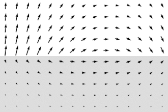
As stated earlier, SPPs are non-radiative. When a SPP travels along a rough surface, it usually becomes radiative due to scattering. The Surface Scattering Theory of light suggests that the scattered intensity per solid angle per incident intensity is[30]


where is the radiation pattern from a single dipole at the metal/dielectric interface. If surface plasmons are excited in the Kretschmann geometry and the scattered light is observed in the plane of incidence (Fig. 4), then the dipole function becomes

![{\displaystyle |W|^{2}=A(\theta ,|\varepsilon _{1}|)\ \sin ^{2}{\psi }\ [(1+\sin ^{2}\theta /|\varepsilon _{1}|)^{1/2}-\sin {\theta }]^{2}}](https://wikimedia.org/api/rest_v1/media/math/render/svg/f5eb62871144241970049eb16996de4aeefb6705)
with

where is the polarization angle and is the angle from the z-axis in the xz-plane. Two important consequences come out of these equations. The first is that if (s-polarization), then and the scattered light . Secondly, the scattered light has a measurable profile which is readily correlated to the roughness. This topic is treated in greater detail in reference.[30]


See also edit
Notes edit
- ^ a b This lossless dispersion relation neglects the effects of damping factors, such as the intrinsic losses in metals. For lossy cases, the dispersion curve backbends after the reaching the surface plasmon frequency instead of asymptotically increasing.[31][32]
References edit
- ^ S.Zeng; Baillargeat, Dominique; Ho, Ho-Pui; Yong, Ken-Tye; et al. (2014). "Nanomaterials enhanced surface plasmon resonance for biological and chemical sensing applications" (PDF). Chemical Society Reviews. 43 (10): 3426–3452. doi:10.1039/C3CS60479A. hdl:10220/18851. PMID 24549396.
- ^ a b c
NIST researchers, Nanofabrication Research Group (2009-08-20). "Three-Dimensional Plasmonic Metamaterials". National Institute of Science and Technology. Retrieved 2011-02-15.
- NIST researchers, Nanofabrication Research Group (2010-02-11). "Opto-mechanical Devices for Measuring Nanoplasmonic Metamaterials". National Institute of Science and Technology. Retrieved 2011-02-15.
 This article incorporates public domain material from Three-Dimensional Plasmonic Metamaterials. National Institute of Standards and Technology.
- ^ Yarris, Lynn (2009-08-20). "GRIN Plasmonics…" (Online news release). U.S. Department of Energy National Laboratory Operated by the University of California. Retrieved 2011-02-15.
- ^
Barnes, William L.; Dereux, Alain; Ebbesen, Thomas W. (2003). "Surface plasmon subwavelength optics". Nature. 424 (6950): 824–30. Bibcode:2003Natur.424..824B. doi:10.1038/nature01937. PMID 12917696. S2CID 116017.
- Huidobro, Paloma A.; Nesterov, Maxim L.; Martín-Moreno, Luis; García-Vidal, Francisco J. (2010). "Transformation Optics for Plasmonics" (PDF). Nano Letters. 10 (6): 1985–90. arXiv:1003.1154. Bibcode:2010NanoL..10.1985H. doi:10.1021/nl100800c. hdl:10044/1/42407. PMID 20465271. S2CID 1255444. Free PDF download for these peer reviewed articles.
- PDF from arxiv.org – Transformation Optics for Plasmonics. 15 pages.
- ^ a b
NIST researchers, Nanofabrication Research Group. "Nanoplasmonics" (Online). National Institute of Science and Technology. Retrieved 2011-02-15.
- This article incorporates public domain material from Nanoplasmonics. National Institute of Standards and Technology.
- ^ Bashevoy, M.V.; Jonsson, F.; Krasavin, A.V.; Zheludev, N.I.; Chen Y.; Stockman M.I. (2006). "Generation of traveling surface plasmon waves by free-electron impact". Nano Letters. 6 (6): 1113–5. arXiv:physics/0604227. Bibcode:2006NanoL...6.1113B. doi:10.1021/nl060941v. PMID 16771563. S2CID 9358094.
- ^ Zeng, Shuwen; Yu, Xia; Law, Wing-Cheung; Zhang, Yating; Hu, Rui; Dinh, Xuan-Quyen; Ho, Ho-Pui; Yong, Ken-Tye (2013). "Size dependence of Au NP-enhanced surface plasmon resonance based on differential phase measurement". Sensors and Actuators B: Chemical. 176: 1128–1133. doi:10.1016/j.snb.2012.09.073.
- ^ a b Raether, Heinz (1988). Surface Plasmons on Smooth and Rough Surfaces and on Gratings. Springer Tracts in Modern Physics 111. New York: Springer-Verlag. ISBN 978-3540173632.
- ^ Cottam, Michael G. (1989). Introduction to Surface and Superlattice Excitations. New York: Cambridge University Press. ISBN 978-0750305884.
- ^ a b Marques Lameirinhas, Ricardo A.; N. Torres, João Paulo; Baptista, António; M. Martins, Maria João. "A new method to analyse the role of surface plasmon polaritons on dielectric-metal interfaces". IEEE Photonics Journal. doi:10.1109/JPHOT.2022.3181967.
- ^ Kittel, Charles (1996). Introduction to Solid State Physics (8th ed.). Hoboken, NJ: John Wiley & Sons. ISBN 978-0-471-41526-8.
- ^ a b Homola, Jirí (2006). Surface Plasmon Resonance Based Sensors. Springer Series on Chemical Sensors and Biosensors, 4. Berlin: Springer-Verlag. ISBN 978-3-540-33918-2.
- ^ Pendry, J. B.; Martín-Moreno, L.; Garcia-Vidal, F. J. (6 August 2004). "Mimicking Surface Plasmons with Structured Surfaces". Science. 305 (5685): 847–848. Bibcode:2004Sci...305..847P. doi:10.1126/science.1098999. PMID 15247438. S2CID 44412157.
- ^ Pan, Bai Cao; Liao, Zhen; Zhao, Jie; Cui, Tie Jun (2014). "Controlling rejections of spoof surface plasmon polaritons using metamaterial particles". Optics Express. 22 (11): 13940–13950. Bibcode:2014OExpr..2213940P. doi:10.1364/OE.22.013940. PMID 24921585.
- ^ Vo-Dinh, Tuan (2017). "Chapter 13 - Biomolecule Sensing Using Surface Plasmon Resonance". Nanotechnology in Biology and Medicine Methods, Devices, and Applications, Second Edition. United States: CRC Press. pp. 259–288. ISBN 978-1439893784.
- ^ Ozbay, E. (2006). "Plasmonics: Merging Photonics and Electronics at Nanoscale Dimensions". Science. 311 (5758): 189–93. Bibcode:2006Sci...311..189O. doi:10.1126/science.1114849. hdl:11693/38263. PMID 16410515. S2CID 2107839.
- ^ Akimov, Yu A; Chu, H S (2012). "Plasmon–plasmon interaction: Controlling light at nanoscale". Nanotechnology. 23 (44): 444004. doi:10.1088/0957-4484/23/44/444004. PMID 23080049. S2CID 5384609.
- ^ Wenshan Cai; Justin S. White & Mark L. Brongersma (2009). "Compact, High-Speed and Power-Efficient Electrooptic Plasmonic Modulators". Nano Letters. 9 (12): 4403–11. Bibcode:2009NanoL...9.4403C. doi:10.1021/nl902701b. PMID 19827771.
- ^ V. K. Valev (2012). "Characterization of Nanostructured Plasmonic Surfaces with Second Harmonic Generation". Langmuir. 28 (44): 15454–15471. doi:10.1021/la302485c. PMID 22889193.
- ^ Minh Hiep, Ha; Endo, Tatsuro; Kerman, Kagan; Chikae, Miyuki; Kim, Do-Kyun; Yamamura, Shohei; Takamura, Yuzuru; Tamiya, Eiichi (2007). "A localized surface plasmon resonance based immunosensor for the detection of casein in milk". Science and Technology of Advanced Materials. 8 (4): 331. Bibcode:2007STAdM...8..331M. doi:10.1016/j.stam.2006.12.010.
- ^ Pochi Yeh (3 March 2005). Optical Waves in Layered Media. Wiley. ISBN 978-0-471-73192-4.
- ^ a b c d West, P.R.; Ishii, S.; Naik, G.V.; Emani, N.K.; Shalaev, V.M.; Boltasseva, A. (2010). "Searching for better plasmonic materials". Laser & Photonics Reviews. 4 (6): 795–808. arXiv:0911.2737. Bibcode:2010LPRv....4..795W. doi:10.1002/lpor.200900055. ISSN 1863-8880. S2CID 16887413.
- ^ Boltasseva, A.; Atwater, H. A. (2011). "Low-Loss Plasmonic Metamaterials". Science. 331 (6015): 290–291. Bibcode:2011Sci...331..290B. doi:10.1126/science.1198258. ISSN 0036-8075. PMID 21252335. S2CID 206530073.
- ^ a b Blaber, M G; Arnold, M D; Ford, M J (2010). "A review of the optical properties of alloys and intermetallics for plasmonics". Journal of Physics: Condensed Matter. 22 (14): 143201. arXiv:1001.4867. Bibcode:2010JPCM...22n3201B. doi:10.1088/0953-8984/22/14/143201. ISSN 0953-8984. PMID 21389523. S2CID 26320849.
- ^ a b c McPeak, Kevin M.; Jayanti, Sriharsha V.; Kress, Stephan J. P.; Meyer, Stefan; Iotti, Stelio; Rossinelli, Aurelio; Norris, David J. (2015). "Plasmonic Films Can Easily Be Better: Rules and Recipes". ACS Photonics. 2 (3): 326–333. doi:10.1021/ph5004237. ISSN 2330-4022. PMC 4416469. PMID 25950012.
- ^ Homola, Jir (2003). "Present and future of surface plasmon resonance biosensors". Analytical and Bioanalytical Chemistry. 377 (3): 528–539. doi:10.1007/s00216-003-2101-0. ISSN 1618-2642. PMID 12879189. S2CID 14370505.
- ^ Etchegoin, P. G.; Le Ru, E. C.; Meyer, M. (2006). "An analytic model for the optical properties of gold". The Journal of Chemical Physics. 125 (16): 164705. Bibcode:2006JChPh.125p4705E. doi:10.1063/1.2360270. ISSN 0021-9606. PMID 17092118.
- ^ Dominici, L; Michelotti, F; Brown, TM; et al. (2009). "Plasmon polaritons in the near infrared on fluorine doped tin oxide films". Optics Express. 17 (12): 10155–67. Bibcode:2009OExpr..1710155D. doi:10.1364/OE.17.010155. PMID 19506669.
- ^ Kretschmann, E. (April 1974). "Die Bestimmung der Oberflächenrauhigkeit dünner Schichten durch Messung der Winkelabhängigkeit der Streustrahlung von Oberflächenplasmaschwingungen". Optics Communications (in German). 10 (4): 353–356. Bibcode:1974OptCo..10..353K. doi:10.1016/0030-4018(74)90362-9.
- ^ a b Kretschmann, E. (1972). "The angular dependence and the polarisation of light emitted by surface plasmons on metals due to roughness". Optics Communications. 5 (5): 331–336. Bibcode:1972OptCo...5..331K. doi:10.1016/0030-4018(72)90026-0.
- ^ Arakawa, E. T.; Williams, M. W.; Hamm, R. N.; Ritchie, R. H. (29 October 1973). "Effect of Damping on Surface Plasmon Dispersion". Physical Review Letters. 31 (18): 1127–1129. Bibcode:1973PhRvL..31.1127A. doi:10.1103/PhysRevLett.31.1127.
- ^ Maier, Stefan A. (2007). Plasmonics: Fundamentals and Applications. New York: Springer Publishing. ISBN 978-0-387-33150-8.
Further reading edit
- Ebbesen, T. W.; Lezec, H. J.; Ghaemi, H. F.; Thio, T.; Wolff, P. A. (1998). "Extraordinary optical transmission through sub-wavelength hole arrays" (PDF). Nature. 391 (6668): 667. Bibcode:1998Natur.391..667E. doi:10.1038/35570. S2CID 205024396.
- Hendry, E.; Garcia-Vidal, F.; Martin-Moreno, L.; Rivas, J.; Bonn, M.; Hibbins, A.; Lockyear, M. (2008). "Optical Control over Surface-Plasmon-Polariton-Assisted THz Transmission through a Slit Aperture" (PDF). Physical Review Letters. 100 (12): 123901. Bibcode:2008PhRvL.100l3901H. doi:10.1103/PhysRevLett.100.123901. hdl:10036/33196. PMID 18517865. Free PDF download.
- Barnes, William L.; Dereux, Alain; Ebbesen, Thomas W. (2003). "Surface plasmon subwavelength optics" (PDF). Nature. 424 (6950): 824–30. Bibcode:2003Natur.424..824B. doi:10.1038/nature01937. PMID 12917696. S2CID 116017. Archived from the original (PDF) on 2011-08-11. Free PDF download.
- Pitarke, J M; Silkin, V M; Chulkov, E V; Echenique, P M (2007). "Theory of surface plasmons and surface-plasmon polaritons" (PDF). Reports on Progress in Physics. 70 (1): 1. arXiv:cond-mat/0611257. Bibcode:2007RPPh...70....1P. doi:10.1088/0034-4885/70/1/R01. S2CID 46471088. Free PDF download.
External links edit
- White, Justin (March 19, 2007). "Surface Plasmon Polaritons" (Online). Stanford University. Physics department. "Submitted as coursework for AP272. Winter 2007".