


Summary
A printed circuit board (PCB), also called printed wiring board (PWB), is a medium used to connect or "wire" components to one another in a circuit. It takes the form of a laminated sandwich structure of conductive and insulating layers: each of the conductive layers is designed with a pattern of traces, planes and other features (similar to wires on a flat surface) etched from one or more sheet layers of copper laminated onto and/or between sheet layers of a non-conductive substrate.[1] Electrical components may be fixed to conductive pads on the outer layers in the shape designed to accept the component's terminals, generally by means of soldering, to both electrically connect and mechanically fasten them to it. Another manufacturing process adds vias, plated-through holes that allow interconnections between layers.
Printed circuit boards are used in nearly all electronic products. Alternatives to PCBs include wire wrap and point-to-point construction, both once popular but now rarely used. PCBs require additional design effort to lay out the circuit, but manufacturing and assembly can be automated. Electronic design automation software is available to do much of the work of layout. Mass-producing circuits with PCBs is cheaper and faster than with other wiring methods, as components are mounted and wired in one operation. Large numbers of PCBs can be fabricated at the same time, and the layout has to be done only once. PCBs can also be made manually in small quantities, with reduced benefits.[2]
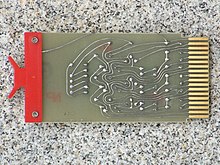
PCBs can be single-sided (one copper layer), double-sided (two copper layers on both sides of one substrate layer), or multi-layer (outer and inner layers of copper, alternating with layers of substrate). Multi-layer PCBs allow for much higher component density, because circuit traces on the inner layers would otherwise take up surface space between components. The rise in popularity of multilayer PCBs with more than two, and especially with more than four, copper planes was concurrent with the adoption of surface mount technology. However, multilayer PCBs make repair, analysis, and field modification of circuits much more difficult and usually impractical.
The world market for bare PCBs exceeded $60.2 billion in 2014[3] and is estimated to reach $79 billion by 2024.[4][5]
History edit
Predecessors edit
Before the development of printed circuit boards, electrical and electronic circuits were wired point-to-point on a chassis. Typically, the chassis was a sheet metal frame or pan, sometimes with a wooden bottom. Components were attached to the chassis, usually by insulators when the connecting point on the chassis was metal, and then their leads were connected directly or with jumper wires by soldering, or sometimes using crimp connectors, wire connector lugs on screw terminals, or other methods. Circuits were large, bulky, heavy, and relatively fragile (even discounting the breakable glass envelopes of the vacuum tubes that were often included in the circuits), and production was labor-intensive, so the products were expensive.
Development of the methods used in modern printed circuit boards started early in the 20th century. In 1903, a German inventor, Albert Hanson, described flat foil conductors laminated to an insulating board, in multiple layers. Thomas Edison experimented with chemical methods of plating conductors onto linen paper in 1904. Arthur Berry in 1913 patented a print-and-etch method in the UK, and in the United States Max Schoop obtained a patent[6] to flame-spray metal onto a board through a patterned mask. Charles Ducas in 1925 patented a method of electroplating circuit patterns.[7]
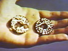
Predating the printed circuit invention, and similar in spirit, was John Sargrove's 1936–1947 Electronic Circuit Making Equipment (ECME) that sprayed metal onto a Bakelite plastic board. The ECME could produce three radio boards per minute.
Early PCBs edit
The Austrian engineer Paul Eisler invented the printed circuit as part of a radio set while working in the UK around 1936. In 1941 a multi-layer printed circuit was used in German magnetic influence naval mines.
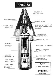
Around 1943 the USA began to use the technology on a large scale to make proximity fuzes for use in World War II.[7] Such fuzes required an electronic circuit that could withstand being fired from a gun, and could be produced in quantity. The Centralab Division of Globe Union submitted a proposal which met the requirements: a ceramic plate would be screenprinted with metallic paint for conductors and carbon material for resistors, with ceramic disc capacitors and subminiature vacuum tubes soldered in place.[8] The technique proved viable, and the resulting patent on the process, which was classified by the U.S. Army, was assigned to Globe Union. It was not until 1984 that the Institute of Electrical and Electronics Engineers (IEEE) awarded Harry W. Rubinstein the Cledo Brunetti Award for early key contributions to the development of printed components and conductors on a common insulating substrate. Rubinstein was honored in 1984 by his alma mater, the University of Wisconsin-Madison, for his innovations in the technology of printed electronic circuits and the fabrication of capacitors.[9][10] This invention also represents a step in the development of integrated circuit technology, as not only wiring but also passive components were fabricated on the ceramic substrate.
Post-war developments edit
In 1948, the USA released the invention for commercial use. Printed circuits did not become commonplace in consumer electronics until the mid-1950s, after the Auto-Sembly process was developed by the United States Army. At around the same time in the UK work along similar lines was carried out by Geoffrey Dummer, then at the RRDE.
Motorola was an early leader in bringing the process into consumer electronics, announcing in August 1952 the adoption of "plated circuits" in home radios after six years of research and a $1M investment.[11] Motorola soon began using its trademarked term for the process, PLAcir, in its consumer radio advertisements.[12] Hallicrafters released its first "foto-etch" printed circuit product, a clock-radio, on 1 November 1952.[13]
Even as circuit boards became available, the point-to-point chassis construction method remained in common use in industry (such as TV and hi-fi sets) into at least the late 1960s. Printed circuit boards were introduced to reduce the size, weight, and cost of parts of the circuitry. In 1960, a small consumer radio receiver might be built with all its circuitry on one circuit board, but a TV set would probably contain one or more circuit boards.
Originally, every electronic component had wire leads, and a PCB had holes drilled for each wire of each component. The component leads were then inserted through the holes and soldered to the copper PCB traces. This method of assembly is called through-hole construction. In 1949, Moe Abramson and Stanislaus F. Danko of the United States Army Signal Corps developed the Auto-Sembly process in which component leads were inserted into a copper foil interconnection pattern and dip soldered. The patent they obtained in 1956 was assigned to the U.S. Army.[14] With the development of board lamination and etching techniques, this concept evolved into the standard printed circuit board fabrication process in use today. Soldering could be done automatically by passing the board over a ripple, or wave, of molten solder in a wave-soldering machine. However, the wires and holes are inefficient since drilling holes is expensive and consumes drill bits and the protruding wires are cut off and discarded.
From the 1980s onward, small surface mount parts have been used increasingly instead of through-hole components; this has led to smaller boards for a given functionality and lower production costs, but with some additional difficulty in servicing faulty boards.
In the 1990s the use of multilayer surface boards became more frequent. As a result, size was further minimized and both flexible and rigid PCBs were incorporated in different devices. In 1995 PCB manufacturers began using microvia technology to produce High-Density Interconnect (HDI) PCBs.[15]
Recent advances edit
Recent advances in 3D printing have meant that there are several new techniques in PCB creation. 3D printed electronics (PEs) can be utilized to print items layer by layer and subsequently the item can be printed with a liquid ink that contains electronic functionalities.
HDI (High Density Interconnect) technology allows for a denser design on the PCB and thus potentially smaller PCBs with more traces and/or components in a given area. As a result, the paths between components can be shorter. HDIs use blind/buried vias, or a combination that includes microvias. With multi-layer HDI PCBs the interconnection of several vias stacked on top of each other (stacked vías, instead of one deep buried via) can be made stronger, thus enhancing reliability in all conditions. The most common applications for HDI technology are computer and mobile phone components as well as medical equipment and military communication equipment. A 4-layer HDI microvia PCB is equivalent in quality to an 8-layer through-hole PCB, so HDI technology can reduce costs. HDI PCBs are often made using build-up film such as ajinomoto build-up film, which is also used in the production of flip chip packages.[16][17] Some PCBs have optical waveguides, similar to optical fibers built on the PCB.[18]
Composition edit

A basic PCB consists of a flat sheet of insulating material and a layer of copper foil, laminated to the substrate. Chemical etching divides the copper into separate conducting lines called tracks or circuit traces, pads for connections, vias to pass connections between layers of copper, and features such as solid conductive areas for electromagnetic shielding or other purposes. The tracks function as wires fixed in place, and are insulated from each other by air and the board substrate material. The surface of a PCB may have a coating that protects the copper from corrosion and reduces the chances of solder shorts between traces or undesired electrical contact with stray bare wires. For its function in helping to prevent solder shorts, the coating is called solder resist or solder mask.
The pattern to be etched into each copper layer of a PCB is called the "artwork". The etching is usually done using photoresist which is coated onto the PCB, then exposed to light projected in the pattern of the artwork. The resist material protects the copper from dissolution into the etching solution. The etched board is then cleaned. A PCB design can be mass-reproduced in a way similar to the way photographs can be mass-duplicated from film negatives using a photographic printer.
FR-4 glass epoxy is the most common insulating substrate. Another substrate material is cotton paper impregnated with phenolic resin, often tan or brown.
When a PCB has no components installed, it is less ambiguously called a printed wiring board (PWB) or etched wiring board.[19] However, the term "printed wiring board" has fallen into disuse. A PCB populated with electronic components is called a printed circuit assembly (PCA), printed circuit board assembly or PCB assembly (PCBA). In informal usage, the term "printed circuit board" most commonly means "printed circuit assembly" (with components). The IPC preferred term for an assembled board is circuit card assembly (CCA),[20] and for an assembled backplane it is backplane assembly. "Card" is another widely used informal term for a "printed circuit assembly". For example, expansion card.
A PCB may be printed with a legend identifying the components, test points, or identifying text. Originally, silkscreen printing was used for this purpose, but today other, finer quality printing methods are usually used. Normally the legend does not affect the function of a PCBA.
Layers edit
A printed circuit board can have multiple layers of copper which almost always are arranged in pairs. The number of layers and the interconnection designed between them (vias, PTHs) provide a general estimate of the board complexity. Using more layers allow for more routing options and better control of signal integrity, but are also time-consuming and costly to manufacture. Likewise, selection of the vias for the board also allow fine tuning of the board size, escaping of signals off complex ICs, routing, and long term reliability, but are tightly coupled with production complexity and cost.
One of the simplest boards to produce is the two-layer board. It has copper on both sides that are referred to as external layers; multi layer boards sandwich additional internal layers of copper and insulation. After two-layer PCBs, the next step up is the four-layer. The four layer board adds significantly more routing options in the internal layers as compared to the two layer board, and often some portion of the internal layers is used as ground plane or power plane, to achieve better signal integrity, higher signaling frequencies, lower EMI, and better power supply decoupling.
In multi-layer boards, the layers of material are laminated together in an alternating sandwich: copper, substrate, copper, substrate, copper, etc.; each plane of copper is etched, and any internal vias (that will not extend to both outer surfaces of the finished multilayer board) are plated-through, before the layers are laminated together. Only the outer layers need be coated; the inner copper layers are protected by the adjacent substrate layers.
Component mounting edit

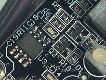
"Through hole" components are mounted by their wire leads passing through the board and soldered to traces on the other side. "Surface mount" components are attached by their leads to copper traces on the same side of the board. A board may use both methods for mounting components. PCBs with only through-hole mounted components are now uncommon. Surface mounting is used for transistors, diodes, IC chips, resistors, and capacitors. Through-hole mounting may be used for some large components such as electrolytic capacitors and connectors.
The first PCBs used through-hole technology, mounting electronic components by leads inserted through holes on one side of the board and soldered onto copper traces on the other side. Boards may be single-sided, with an unplated component side, or more compact double-sided boards, with components soldered on both sides. Horizontal installation of through-hole parts with two axial leads (such as resistors, capacitors, and diodes) is done by bending the leads 90 degrees in the same direction, inserting the part in the board (often bending leads located on the back of the board in opposite directions to improve the part's mechanical strength), soldering the leads, and trimming off the ends. Leads may be soldered either manually or by a wave soldering machine.[21] Through-hole manufacture adds to board cost by requiring many holes to be drilled accurately, and it limits the available routing area for signal traces on layers immediately below the top layer on multi-layer boards, since the holes must pass through all layers to the opposite side. Once surface-mounting came into use, small-sized SMD components were used where possible, with through-hole mounting only of components unsuitably large for surface-mounting due to power requirements or mechanical limitations, or subject to mechanical stress which might damage the PCB (e.g. by lifting the copper off the board surface).[citation needed]
Surface-mount technology emerged in the 1960s, gained momentum in the early 1980s, and became widely used by the mid-1990s. Components were mechanically redesigned to have small metal tabs or end caps that could be soldered directly onto the PCB surface, instead of wire leads to pass through holes. Components became much smaller and component placement on both sides of the board became more common than with through-hole mounting, allowing much smaller PCB assemblies with much higher circuit densities. Surface mounting lends itself well to a high degree of automation, reducing labor costs and greatly increasing production rates compared with through-hole circuit boards. Components can be supplied mounted on carrier tapes. Surface mount components can be about one-quarter to one-tenth of the size and weight of through-hole components, and passive components much cheaper. However, prices of semiconductor surface mount devices (SMDs) are determined more by the chip itself than the package, with little price advantage over larger packages, and some wire-ended components, such as 1N4148 small-signal switch diodes, are actually significantly cheaper than SMD equivalents.
Electrical properties edit
Each trace consists of a flat, narrow part of the copper foil that remains after etching. Its resistance, determined by its width, thickness, and length, must be sufficiently low for the current the conductor will carry. Power and ground traces may need to be wider than signal traces. In a multi-layer board one entire layer may be mostly solid copper to act as a ground plane for shielding and power return. For microwave circuits, transmission lines can be laid out in a planar form such as stripline or microstrip with carefully controlled dimensions to assure a consistent impedance. In radio-frequency and fast switching circuits the inductance and capacitance of the printed circuit board conductors become significant circuit elements, usually undesired; conversely, they can be used as a deliberate part of the circuit design, as in distributed-element filters, antennae, and fuses, obviating the need for additional discrete components. High density interconnects (HDI) PCBs have tracks and/or vias with a width or diameter of under 152 micrometers.[22]
Materials edit
Laminates edit
Laminates are manufactured by curing layers of cloth or paper with thermoset resin under pressure and heat to form an integral final piece of uniform thickness. They can be up to 4 by 8 feet (1.2 by 2.4 m) in width and length. Varying cloth weaves (threads per inch or cm), cloth thickness, and resin percentage are used to achieve the desired final thickness and dielectric characteristics. Available standard laminate thickness are listed in ANSI/IPC-D-275.[23]
The cloth or fiber material used, resin material, and the cloth to resin ratio determine the laminate's type designation (FR-4, CEM-1, G-10, etc.) and therefore the characteristics of the laminate produced. Important characteristics are the level to which the laminate is fire retardant, the dielectric constant (er), the loss tangent (tan δ), the tensile strength, the shear strength, the glass transition temperature (Tg), and the Z-axis expansion coefficient (how much the thickness changes with temperature).
There are quite a few different dielectrics that can be chosen to provide different insulating values depending on the requirements of the circuit. Some of these dielectrics are polytetrafluoroethylene (Teflon), FR-4, FR-1, CEM-1 or CEM-3. Well known pre-preg materials used in the PCB industry are FR-2 (phenolic cotton paper), FR-3 (cotton paper and epoxy), FR-4 (woven glass and epoxy), FR-5 (woven glass and epoxy), FR-6 (matte glass and polyester), G-10 (woven glass and epoxy), CEM-1 (cotton paper and epoxy), CEM-2 (cotton paper and epoxy), CEM-3 (non-woven glass and epoxy), CEM-4 (woven glass and epoxy), CEM-5 (woven glass and polyester). Thermal expansion is an important consideration especially with ball grid array (BGA) and naked die technologies, and glass fiber offers the best dimensional stability.
FR-4 is by far the most common material used today. The board stock with unetched copper on it is called "copper-clad laminate".
With decreasing size of board features and increasing frequencies, small nonhomogeneities like uneven distribution of fiberglass or other filler, thickness variations, and bubbles in the resin matrix, and the associated local variations in the dielectric constant, are gaining importance.
Key substrate parameters edit
The circuitboard substrates are usually dielectric composite materials. The composites contain a matrix (usually an epoxy resin) and a reinforcement (usually a woven, sometimes nonwoven, glass fibers, sometimes even paper), and in some cases a filler is added to the resin (e.g. ceramics; titanate ceramics can be used to increase the dielectric constant).
The reinforcement type defines two major classes of materials: woven and non-woven. Woven reinforcements are cheaper, but the high dielectric constant of glass may not be favorable for many higher-frequency applications. The spatially nonhomogeneous structure also introduces local variations in electrical parameters, due to different resin/glass ratio at different areas of the weave pattern. Nonwoven reinforcements, or materials with low or no reinforcement, are more expensive but more suitable for some RF/analog applications.
The substrates are characterized by several key parameters, chiefly thermomechanical (glass transition temperature, tensile strength, shear strength, thermal expansion), electrical (dielectric constant, loss tangent, dielectric breakdown voltage, leakage current, tracking resistance...), and others (e.g. moisture absorption).
At the glass transition temperature the resin in the composite softens and significantly increases thermal expansion; exceeding Tg then exerts mechanical overload on the board components - e.g. the joints and the vias. Below Tg the thermal expansion of the resin roughly matches copper and glass, above it gets significantly higher. As the reinforcement and copper confine the board along the plane, virtually all volume expansion projects to the thickness and stresses the plated-through holes. Repeated soldering or other exposition to higher temperatures can cause failure of the plating, especially with thicker boards; thick boards therefore require a matrix with a high Tg.
The materials used determine the substrate's dielectric constant. This constant is also dependent on frequency, usually decreasing with frequency. As this constant determines the signal propagation speed, frequency dependence introduces phase distortion in wideband applications; as flat a dielectric constant vs frequency characteristics as is achievable is important here. The impedance of transmission lines decreases with frequency, therefore faster edges of signals reflect more than slower ones.
Dielectric breakdown voltage determines the maximum voltage gradient the material can be subjected to before suffering a breakdown (conduction, or arcing, through the dielectric).
Tracking resistance determines how the material resists high voltage electrical discharges creeping over the board surface.
Loss tangent determines how much of the electromagnetic energy from the signals in the conductors is absorbed in the board material. This factor is important for high frequencies. Low-loss materials are more expensive. Choosing unnecessarily low-loss material is a common engineering error in high-frequency digital design; it increases the cost of the boards without a corresponding benefit. Signal degradation by loss tangent and dielectric constant can be easily assessed by an eye pattern.
Moisture absorption occurs when the material is exposed to high humidity or water. Both the resin and the reinforcement may absorb water; water also may be soaked by capillary forces through voids in the materials and along the reinforcement. Epoxies of the FR-4 materials are not too susceptible, with absorption of only 0.15%. Teflon has very low absorption of 0.01%. Polyimides and cyanate esters, on the other side, suffer from high water absorption. Absorbed water can lead to significant degradation of key parameters; it impairs tracking resistance, breakdown voltage, and dielectric parameters. Relative dielectric constant of water is about 73, compared to about 4 for common circuit board materials. Absorbed moisture can also vaporize on heating, as during soldering, and cause cracking and delamination,[24] the same effect responsible for "popcorning" damage on wet packaging of electronic parts. Careful baking of the substrates may be required to dry them prior to soldering.[25]
Common substrates edit
Often encountered materials:
- FR-2, phenolic paper or phenolic cotton paper, paper impregnated with a phenol formaldehyde resin. Common in consumer electronics with single-sided boards. Electrical properties inferior to FR-4. Poor arc resistance. Generally rated to 105 °C.
- FR-4, a woven fiberglass cloth impregnated with an epoxy resin. Low water absorption (up to about 0.15%), good insulation properties, good arc resistance. Very common. Several grades with somewhat different properties are available. Typically rated to 130 °C.
- Aluminum, or metal core board or insulated metal substrate (IMS), clad with thermally conductive thin dielectric - used for parts requiring significant cooling - power switches, LEDs. Consists of usually single, sometimes double layer thin circuit board based on e.g. FR-4, laminated on aluminum sheet metal, commonly 0.8, 1, 1.5, 2 or 3 mm thick. The thicker laminates sometimes also come with thicker copper metalization.[26][27]
- Flexible substrates - can be a standalone copper-clad foil or can be laminated to a thin stiffener, e.g. 50-130 µm
- Kapton or UPILEX,[28] a polyimide foil. Used for flexible printed circuits, in this form common in small form-factor consumer electronics or for flexible interconnects. Resistant to high temperatures.
- Pyralux, a polyimide-fluoropolymer composite foil.[29] Copper layer can delaminate during soldering.
Less-often encountered materials:
- FR-1, like FR-2, typically specified to 105 °C, some grades rated to 130 °C. Room-temperature punchable. Similar to cardboard. Poor moisture resistance. Low arc resistance.
- FR-3, cotton paper impregnated with epoxy. Typically rated to 105 °C.
- FR-5, woven fiberglass and epoxy, high strength at higher temperatures, typically specified to 170 °C.
- FR-6, matte glass and polyester
- G-10, woven glass and epoxy - high insulation resistance, low moisture absorption, very high bond strength. Typically rated to 130 °C.
- G-11, woven glass and epoxy - high resistance to solvents, high flexural strength retention at high temperatures.[30] Typically rated to 170 °C.
- CEM-1, cotton paper and epoxy
- CEM-2, cotton paper and epoxy
- CEM-3, non-woven glass and epoxy
- CEM-4, woven glass and epoxy
- CEM-5, woven glass and polyester
- PTFE, ("Teflon") - expensive, low dielectric loss, for high frequency applications, very low moisture absorption (0.01%), mechanically soft. Difficult to laminate, rarely used in multilayer applications.
- PTFE, ceramic filled - expensive, low dielectric loss, for high frequency applications. Varying ceramics/PTFE ratio allows adjusting dielectric constant and thermal expansion.
- RF-35, fiberglass-reinforced ceramics-filled PTFE. Relatively less expensive, good mechanical properties, good high-frequency properties.[31][32]
- Alumina, a ceramic. Hard, brittle, very expensive, very high performance, good thermal conductivity.
- Polyimide, a high-temperature polymer. Expensive, high-performance. Higher water absorption (0.4%). Can be used from cryogenic temperatures to over 260 °C.
Copper thickness edit
Copper thickness of PCBs can be specified directly or as the weight of copper per area (in ounce per square foot) which is easier to measure. One ounce per square foot is 1.344 mils or 34 micrometers thickness. Heavy copper is a layer exceeding three ounces of copper per ft2, or approximately 0.0042 inches (4.2 mils, 105 μm) thick. Heavy copper layers are used for high current or to help dissipate heat.
On the common FR-4 substrates, 1 oz copper per ft2 (35 µm) is the most common thickness; 2 oz (70 µm) and 0.5 oz (17.5 µm) thickness is often an option. Less common are 12 and 105 µm, 9 µm is sometimes available on some substrates. Flexible substrates typically have thinner metalization. Metal-core boards for high power devices commonly use thicker copper; 35 µm is usual but also 140 and 400 µm can be encountered.
In the US, copper foil thickness is specified in units of ounces per square foot (oz/ft2), commonly referred to simply as ounce. Common thicknesses are 1/2 oz/ft2 (150 g/m2), 1 oz/ft2 (300 g/m2), 2 oz/ft2 (600 g/m2), and 3 oz/ft2 (900 g/m2). These work out to thicknesses of 17.05 μm (0.67 thou), 34.1 μm (1.34 thou), 68.2 μm (2.68 thou), and 102.3 μm (4.02 thou), respectively.
| oz/ft2 | g/m2 | μm | thou |
|---|---|---|---|
| 1/2 oz/ft2 | 150 g/m2 | 17.05 μm | 0.67 thou |
| 1 oz/ft2 | 300 g/m2 | 34.1 μm | 1.34 thou |
| 2 oz/ft2 | 600 g/m2 | 68.2 μm | 2.68 thou |
| 3 oz/ft2 | 900 g/m2 | 102.3 μm | 4.02 thou |
1/2 oz/ft2 foil is not widely used as a finished copper weight, but is used for outer layers when plating for through holes will increase the finished copper weight Some PCB manufacturers refer to 1 oz/ft2 copper foil as having a thickness of 35 μm (may also be referred to as 35 μ, 35 micron, or 35 mic).
- 1/0 – denotes 1 oz/ft2 copper one side, with no copper on the other side.
- 1/1 – denotes 1 oz/ft2 copper on both sides.
- H/0 or H/H – denotes 0.5 oz/ft2 copper on one or both sides, respectively.
- 2/0 or 2/2 – denotes 2 oz/ft2 copper on one or both sides, respectively.
Construction edit
Design edit
Manufacturing starts from the fabrication data generated by computer aided design, and component information. The fabrication data is read into the CAM (Computer Aided Manufacturing) software. CAM performs the following functions:
- Input of the fabrication data.
- Verification of the data
- Compensation for deviations in the manufacturing processes (e.g. scaling to compensate for distortions during lamination)
- Panelization
- Output of the digital tools (copper patterns, drill files, inspection, and others)
Initially PCBs were designed manually by creating a photomask on a clear mylar sheet, usually at two or four times the true size. Starting from the schematic diagram the component pin pads were laid out on the mylar and then traces were routed to connect the pads. Rub-on dry transfers of common component footprints increased efficiency. Traces were made with self-adhesive tape. Pre-printed non-reproducing grids on the mylar assisted in layout. The finished photomask was photolithographically reproduced onto a photoresist coating on the blank copper-clad boards.
Modern PCBs are designed with dedicated layout software, generally in the following steps:[33][34]
- Schematic capture through an electronic design automation (EDA) tool.
- Card dimensions and template are decided based on required circuitry and enclosure of the PCB.
- The positions of the components and heat sinks are determined.
- Layer stack of the PCB is decided, with one to tens of layers depending on complexity. Ground and power planes are decided. A power plane is the counterpart to a ground plane and behaves as an AC signal ground while providing DC power to the circuits mounted on the PCB. Signal interconnections are traced on signal planes. Signal planes can be on the outer as well as inner layers. For optimal EMI performance high frequency signals are routed in internal layers between power or ground planes.[35]
- Line impedance is determined using dielectric layer thickness, routing copper thickness and trace-width. Trace separation is also taken into account in case of differential signals. Microstrip, stripline or dual stripline can be used to route signals.
- Components are placed. Thermal considerations and geometry are taken into account. Vias and lands are marked.
- Signal traces are routed. Electronic design automation tools usually create clearances and connections in power and ground planes automatically.
- Fabrication data consists of a set of Gerber files, a drill file, and a pick-and-place file.[34]
Panelization edit
Several small printed circuit boards can be grouped together for processing as a panel. A panel consisting of a design duplicated n-times is also called an n-panel, whereas a multi-panel combines several different designs onto a single panel. The outer tooling strip often includes tooling holes, a set of panel fiducials, a test coupon, and may include hatched copper pour or similar patterns for even copper distribution over the whole panel in order to avoid bending. The assemblers often mount components on panels rather than single PCBs because this is efficient. Panelization may also be necessary for boards with components placed near an edge of the board because otherwise the board could not be mounted during assembly. Most assembly shops require a free area of at least 10 mm around the board.
Depaneling edit
The panel is eventually broken into individual PCBs along perforations or grooves in the panel[36] through milling or cutting. For milled panels a common distance between the individual boards is 2–3 mm. Today depaneling is often done by lasers which cut the board with no contact. Laser depaneling reduces stress on the fragile circuits, improving the yield of defect-free units.
Copper patterning edit
The first step is to replicate the pattern in the fabricator's CAM system on a protective mask on the copper foil PCB layers. Subsequent etching removes the unwanted copper unprotected by the mask. (Alternatively, a conductive ink can be ink-jetted on a blank (non-conductive) board. This technique is also used in the manufacture of hybrid circuits.)
- Silk screen printing uses etch-resistant inks to create the protective mask.
- Photoengraving uses a photomask and developer to selectively remove a UV-sensitive photoresist coating and thus create a photoresist mask that will protect the copper below it. Direct imaging techniques are sometimes used for high-resolution requirements. Experiments have been made with thermal resist.[37] A laser may be used instead of a photomask. This is known as maskless lithography or direct imaging.
- PCB milling uses a two or three-axis mechanical milling system to mill away the copper foil from the substrate. A PCB milling machine (referred to as a 'PCB Prototyper') operates in a similar way to a plotter, receiving commands from the host software that control the position of the milling head in the x, y, and (if relevant) z axis.
- Laser resist ablation Spray black paint onto copper clad laminate, place into CNC laser plotter. The laser raster-scans the PCB and ablates (vaporizes) the paint where no resist is wanted. (Note: laser copper ablation is rarely used and is considered experimental.[clarification needed])
- Laser etching The copper may be removed directly by a CNC laser. Like PCB milling above this is used mainly for prototyping.
- EDM etching uses an electrical discharge to remove a metal from a substrate submerged into a dielectric fluid
The method chosen depends on the number of boards to be produced and the required resolution.
- Large volume
- Silk screen printing – Used for PCBs with bigger features
- Photoengraving – Used when finer features are required
- Small volume
- Print onto transparent film and use as photo mask along with photo-sensitized boards, then etch. (Alternatively, use a film photoplotter)
- Laser resist ablation
- PCB milling
- Laser etching
- Hobbyist
- Laser-printed resist: Laser-print onto toner transfer paper, heat-transfer with an iron or modified laminator onto bare laminate, soak in water bath, touch up with a marker, then etch.
- Vinyl film and resist, non-washable marker, some other methods. Labor-intensive, only suitable for single boards.
Etching edit

The process by which copper traces are applied to the surface is known as etching after the subtractive method of the process, though there are also additive and semi-additive methods.
Subtractive methods remove copper from an entirely copper-coated board to leave only the desired copper pattern. The simplest method, used for small-scale production and often by hobbyists, is immersion etching, in which the board is submerged in etching solution such as ferric chloride. Compared with methods used for mass production, the etching time is long. Heat and agitation can be applied to the bath to speed the etching rate. In bubble etching, air is passed through the etchant bath to agitate the solution and speed up etching. Splash etching uses a motor-driven paddle to splash boards with etchant; the process has become commercially obsolete since it is not as fast as spray etching. In spray etching, the etchant solution is distributed over the boards by nozzles, and recirculated by pumps. Adjustment of the nozzle pattern, flow rate, temperature, and etchant composition gives predictable control of etching rates and high production rates.[38] As more copper is consumed from the boards, the etchant becomes saturated and less effective; different etchants have different capacities for copper, with some as high as 150 grams of copper per liter of solution. In commercial use, etchants can be regenerated to restore their activity, and the dissolved copper recovered and sold. Small-scale etching requires attention to disposal of used etchant, which is corrosive and toxic due to its metal content.[39] The etchant removes copper on all surfaces not protected by the resist. "Undercut" occurs when etchant attacks the thin edge of copper under the resist; this can reduce conductor widths and cause open-circuits. Careful control of etch time is required to prevent undercut. Where metallic plating is used as a resist, it can "overhang" which can cause short-circuits between adjacent traces when closely spaced. Overhang can be removed by wire-brushing the board after etching.[38]
In additive methods the pattern is electroplated onto a bare substrate using a complex process. The advantage of the additive method is that less material is needed and less waste is produced. In the full additive process the bare laminate is covered with a photosensitive film which is imaged (exposed to light through a mask and then developed which removes the unexposed film). The exposed areas are sensitized in a chemical bath, usually containing palladium and similar to that used for through hole plating which makes the exposed area capable of bonding metal ions. The laminate is then plated with copper in the sensitized areas. When the mask is stripped, the PCB is finished.
Semi-additive is the most common process: The unpatterned board has a thin layer of copper already on it. A reverse mask is then applied (Unlike a subtractive process mask, this mask exposes those parts of the substrate that will eventually become the traces). Additional copper is then plated onto the board in the unmasked areas; copper may be plated to any desired weight. Tin-lead or other surface platings are then applied. The mask is stripped away and a brief etching step removes the now-exposed bare original copper laminate from the board, isolating the individual traces. Some single-sided boards which have plated-through holes are made in this way. General Electric made consumer radio sets in the late 1960s using additive boards. The (semi-)additive process is commonly used for multi-layer boards as it facilitates the plating-through of the holes to produce conductive vias in the circuit board.
Industrial etching is usually done with ammonium persulfate or ferric chloride. For PTH (plated-through holes), additional steps of electroless deposition are done after the holes are drilled, then copper is electroplated to build up the thickness, the boards are screened, and plated with tin/lead. The tin/lead becomes the resist leaving the bare copper to be etched away.[40]
Lamination edit
Multi-layer printed circuit boards have trace layers inside the board. This is achieved by laminating a stack of materials in a press by applying pressure and heat for a period of time. This results in an inseparable one piece product. For example, a four-layer PCB can be fabricated by starting from a two-sided copper-clad laminate, etch the circuitry on both sides, then laminate to the top and bottom pre-preg and copper foil. It is then drilled, plated, and etched again to get traces on top and bottom layers.[41]
The inner layers are given a complete machine inspection before lamination because mistakes cannot be corrected afterwards. Automatic optical inspection (AOI) machines compare an image of the board with the digital image generated from the original design data. Automated Optical Shaping (AOS) machines can then add missing copper or remove excess copper using a laser, reducing the number of PCBs that have to be discarded.[42][43][44] PCB tracks can have a width of just 10 micrometers.
Drilling edit
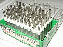
Holes through a PCB are typically drilled with drill bits coated with tungsten carbide. Coated tungsten carbide is used because board materials are abrasive. High-speed-steel bits would dull quickly, tearing the copper and ruining the board. Drilling is done by computer-controlled drilling machines, using a drill file or Excellon file that describes the location and size of each drilled hole.
Vias edit
Holes may be made conductive, by electroplating or inserting hollow metal eyelets, to connect board layers. Some conductive holes are intended for the insertion of through-hole-component leads. Others used to connect board layers, are called vias.
Micro vias edit
When vias with a diameter smaller than 76.2 micrometers are required, drilling with mechanical bits is impossible because of high rates of wear and breakage. In this case, the vias may be laser drilled—evaporated by lasers. Laser-drilled vias typically have an inferior surface finish inside the hole. These holes are called micro vias and can have diameters as small as 10 micrometers.[45][46]
Blind and buried vias edit
It is also possible with controlled-depth drilling, laser drilling, or by pre-drilling the individual sheets of the PCB before lamination, to produce holes that connect only some of the copper layers, rather than passing through the entire board. These holes are called blind vias when they connect an internal copper layer to an outer layer, or buried vias when they connect two or more internal copper layers and no outer layers. Laser drilling machines can drill thousands of holes per second and can use either UV or CO2 lasers.[47][48]
The hole walls for boards with two or more layers can be made conductive and then electroplated with copper to form plated-through holes. These holes electrically connect the conducting layers of the PCB.
Smear edit
For multi-layer boards, those with three layers or more, drilling typically produces a smear of the high temperature decomposition products of bonding agent in the laminate system. Before the holes can be plated through, this smear must be removed by a chemical de-smear process, or by Plasma etching. The de-smear process ensures that a good connection is made to the copper layers when the hole is plated through. On high reliability boards a process called etch-back is performed chemically with a potassium permanganate based etchant or plasma etching. The etch-back removes resin and the glass fibers so that the copper layers extend into the hole and as the hole is plated become integral with the deposited copper.
Plating and coating edit
Proper plating or surface finish selection can be critical to process yield, the amount of rework, field failure rate, and reliability.[49]
PCBs may be plated with solder, tin, or gold over nickel.[50][51]
After PCBs are etched and then rinsed with water, the solder mask is applied, and then any exposed copper is coated with solder, nickel/gold, or some other anti-corrosion coating.[52]
Matte solder is usually fused to provide a better bonding surface for bare copper. Treatments, such as benzimidazolethiol, prevent surface oxidation of bare copper. The places to which components will be mounted are typically plated, because untreated bare copper oxidizes quickly, and therefore is not readily solderable. Traditionally, any exposed copper was coated with solder by hot air (solder) levelling (HASL aka HAL). The HASL finish prevents oxidation from the underlying copper, thereby guaranteeing a solderable surface. This solder was a tin-lead alloy, however new solder compounds are now used to achieve compliance with the RoHS directive in the EU, which restricts the use of lead. One of these lead-free compounds is SN100CL, made up of 99.3% tin, 0.7% copper, 0.05% nickel, and a nominal of 60 ppm germanium.[citation needed]
It is important to use solder compatible with both the PCB and the parts used. An example is ball grid array (BGA) using tin-lead solder balls for connections losing their balls on bare copper traces or using lead-free solder paste.
Other platings used are organic solderability preservative (OSP), immersion silver (IAg), immersion tin (ISn), electroless nickel immersion gold (ENIG) coating, electroless nickel electroless palladium immersion gold (ENEPIG), and direct gold plating (over nickel). Edge connectors, placed along one edge of some boards, are often nickel-plated then gold-plated using ENIG. Another coating consideration is rapid diffusion of coating metal into tin solder. Tin forms intermetallics such as Cu6Sn5 and Ag3Cu that dissolve into the Tin liquidus or solidus (at 50 °C), stripping surface coating or leaving voids.
Electrochemical migration (ECM) is the growth of conductive metal filaments on or in a printed circuit board (PCB) under the influence of a DC voltage bias.[53][54] Silver, zinc, and aluminum are known to grow whiskers under the influence of an electric field. Silver also grows conducting surface paths in the presence of halide and other ions, making it a poor choice for electronics use. Tin will grow "whiskers" due to tension in the plated surface. Tin-lead or solder plating also grows whiskers, only reduced by reducing the percentage of tin. Reflow to melt solder or tin plate to relieve surface stress lowers whisker incidence. Another coating issue is tin pest, the transformation of tin to a powdery allotrope at low temperature.[55]
Solder resist application edit
Areas that should not be soldered may be covered with solder resist (solder mask). The solder mask is what gives PCBs their characteristic green color, although it is also available in several other colors, such as red, blue, purple, yellow, black and white. One of the most common solder resists used today is called "LPI" (liquid photoimageable solder mask).[56] A photo-sensitive coating is applied to the surface of the PWB, then exposed to light through the solder mask image film, and finally developed where the unexposed areas are washed away. Dry film solder mask is similar to the dry film used to image the PWB for plating or etching. After being laminated to the PWB surface it is imaged and developed as LPI. Once but no longer commonly used, because of its low accuracy and resolution, is to screen print epoxy ink. In addition to repelling solder, solder resist also provides protection from the environment to the copper that would otherwise be exposed.
Legend / silkscreen edit
A legend (also known as silk or silkscreen) is often printed on one or both sides of the PCB. It contains the component designators, switch settings, test points and other indications helpful in assembling, testing, servicing, and sometimes using the circuit board.
There are three methods to print the legend:
- Silkscreen printing epoxy ink was the established method, resulting in the alternative name.
- Liquid photo imaging is a more accurate method than screen printing.
- Ink jet printing is increasingly used. Ink jet can print variable data, unique to each PWB unit, such as text or a bar code with a serial number.
Bare-board test edit
Boards with no components installed are usually bare-board tested for "shorts" and "opens". This is called electrical test or PCB e-test. A short is a connection between two points that should not be connected. An open is a missing connection between points that should be connected. For high-volume production, a fixture such as a "bed of nails" in a rigid needle adapter makes contact with copper lands on the board. The fixture or adapter is a significant fixed cost and this method is only economical for high-volume or high-value production. For small or medium volume production flying probe testers are used where test probes are moved over the board by an XY drive to make contact with the copper lands. There is no need for a fixture and hence the fixed costs are much lower. The CAM system instructs the electrical tester to apply a voltage to each contact point as required and to check that this voltage appears on the appropriate contact points and only on these.
Assembly edit

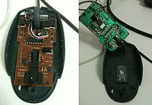
In assembly the bare board is populated (or "stuffed") with electronic components to form a functional printed circuit assembly (PCA), sometimes called a "printed circuit board assembly" (PCBA).[57][58] In through-hole technology, the component leads are inserted in holes surrounded by conductive pads; the holes keep the components in place. In surface-mount technology (SMT), the component is placed on the PCB so that the pins line up with the conductive pads or lands on the surfaces of the PCB; solder paste, which was previously applied to the pads, holds the components in place temporarily; if surface-mount components are applied to both sides of the board, the bottom-side components are glued to the board. In both through hole and surface mount, the components are then soldered; once cooled and solidified, the solder holds the components in place permanently and electrically connects them to the board.
There are a variety of soldering techniques used to attach components to a PCB. High volume production is usually done with a pick-and-place machine and bulk wave soldering for through-hole parts or reflow ovens for SMT components and/or through-hole parts, but skilled technicians are able to hand-solder very tiny parts (for instance 0201 packages which are 0.02 in. by 0.01 in.)[59] under a microscope, using tweezers and a fine-tip soldering iron, for small volume prototypes. Selective soldering may be used for delicate parts. Some SMT parts cannot be soldered by hand, such as BGA packages. All through-hole components can be hand soldered, making them favored for prototyping where size, weight, and the use of the exact components that would be used in high volume production are not concerns.
Often, through-hole and surface-mount construction must be combined in a single assembly because some required components are available only in surface-mount packages, while others are available only in through-hole packages. Or, even if all components are available in through-hole packages, it might be desired to take advantage of the size, weight, and cost reductions obtainable by using some available surface-mount devices. Another reason to use both methods is that through-hole mounting can provide needed strength for components likely to endure physical stress (such as connectors that are frequently mated and demated or that connect to cables expected to impart substantial stress to the PCB-and-connector interface), while components that are expected to go untouched will take up less space using surface-mount techniques. For further comparison, see the SMT page.
After the board has been populated it may be tested in a variety of ways:
- While the power is off, visual inspection, automated optical inspection. JEDEC guidelines for PCB component placement, soldering, and inspection are commonly used to maintain quality control in this stage of PCB manufacturing.
- While the power is off, analog signature analysis, power-off testing.
- While the power is on, in-circuit test, where physical measurements (for example, voltage) can be done.
- While the power is on, functional test, just checking if the PCB does what it had been designed to do.
To facilitate these tests, PCBs may be designed with extra pads to make temporary connections. Sometimes these pads must be isolated with resistors. The in-circuit test may also exercise boundary scan test features of some components. In-circuit test systems may also be used to program nonvolatile memory components on the board.
In boundary scan testing, test circuits integrated into various ICs on the board form temporary connections between the PCB traces to test that the ICs are mounted correctly. Boundary scan testing requires that all the ICs to be tested use a standard test configuration procedure, the most common one being the Joint Test Action Group (JTAG) standard. The JTAG test architecture provides a means to test interconnects between integrated circuits on a board without using physical test probes, by using circuitry in the ICs to employ the IC pins themselves as test probes. JTAG tool vendors provide various types of stimuli and sophisticated algorithms, not only to detect the failing nets, but also to isolate the faults to specific nets, devices, and pins.
When boards fail the test, technicians may desolder and replace failed components, a task known as rework.
Protection and packaging edit
PCBs intended for extreme environments often have a conformal coating, which is applied by dipping or spraying after the components have been soldered. The coat prevents corrosion and leakage currents or shorting due to condensation. The earliest conformal coats were wax; modern conformal coats are usually dips of dilute solutions of silicone rubber, polyurethane, acrylic, or epoxy. Another technique for applying a conformal coating is for plastic to be sputtered onto the PCB in a vacuum chamber. The chief disadvantage of conformal coatings is that servicing of the board is rendered extremely difficult.[60]
Many assembled PCBs are static sensitive, and therefore they must be placed in antistatic bags during transport. When handling these boards, the user must be grounded (earthed). Improper handling techniques might transmit an accumulated static charge through the board, damaging or destroying components. The damage might not immediately affect function but might lead to early failure later on, cause intermittent operating faults, or cause a narrowing of the range of environmental and electrical conditions under which the board functions properly. Even bare boards are sometimes static sensitive: traces have become so fine that it is possible to blow a trace (or change its characteristics) with a static discharge. This is especially true on non-traditional PCBs such as MCMs and microwave PCBs.
Cordwood construction edit

Cordwood construction can save significant space and was often used with wire-ended components in applications where space was at a premium (such as fuzes, missile guidance, and telemetry systems) and in high-speed computers, where short traces were important. In cordwood construction, axial-leaded components were mounted between two parallel planes. The name comes from the way axial-lead components (capacitors, resistors, coils, and diodes) are stacked in parallel rows and columns, like a stack of firewood. The components were either soldered together with jumper wire or they were connected to other components by thin nickel ribbon welded at right angles onto the component leads.[61] To avoid shorting together different interconnection layers, thin insulating cards were placed between them. Perforations or holes in the cards allowed component leads to project through to the next interconnection layer. One disadvantage of this system was that special nickel-leaded components had to be used to allow reliable interconnecting welds to be made. Differential thermal expansion of the component could put pressure on the leads of the components and the PCB traces and cause mechanical damage (as was seen in several modules on the Apollo program). Additionally, components located in the interior are difficult to replace. Some versions of cordwood construction used soldered single-sided PCBs as the interconnection method (as pictured), allowing the use of normal-leaded components at the cost of being difficult to remove the boards or replace any component that is not at the edge.
Before the advent of integrated circuits, this method allowed the highest possible component packing density; because of this, it was used by a number of computer vendors including Control Data Corporation. The cordwood method of construction was used only rarely once PCBs became widespread, mainly in aerospace or other extremely high-density electronics.
Types edit
Breakout boards edit
A minimal PCB for a single component, used for prototyping, is called a breakout board. The purpose of a breakout board is to "break out" the leads of a component on separate terminals so that manual connections to them can be made easily. Breakout boards are especially used for surface-mount components or any components with fine lead pitch.
Advanced PCBs may contain components embedded in the substrate, such as capacitors and integrated circuits, to reduce the amount of space taken up by components on the surface of the PCB while improving electrical characteristics.[62]
Multiwire boards edit
Multiwire is a patented technique of interconnection which uses machine-routed insulated wires embedded in a non-conducting matrix (often plastic resin).[63] It was used during the 1980s and 1990s. As of 2010, Multiwire was still available through Hitachi.
Since it was quite easy to stack interconnections (wires) inside the embedding matrix, the approach allowed designers to forget completely about the routing of wires (usually a time-consuming operation of PCB design): Anywhere the designer needs a connection, the machine will draw a wire in a straight line from one location/pin to another. This led to very short design times (no complex algorithms to use even for high density designs) as well as reduced crosstalk (which is worse when wires run parallel to each other—which almost never happens in Multiwire), though the cost is too high to compete with cheaper PCB technologies when large quantities are needed.
Corrections can be made to a Multiwire board layout more easily than to a PCB layout.[64]
Uses edit
Printed circuit boards have been used as an alternative to their typical use for electronic and biomedical engineering thanks to the versatility of their layers, especially the copper layer. PCB layers have been used to fabricate sensors, such as capacitive pressure sensors and accelerometers, actuators such as microvalves and microheaters, as well as platforms of sensors and actuators for Lab-on-a-chip (LoC), for example to perform polymerase chain reaction (PCR), and fuel cells, to name a few.[65]
Repair edit
Manufacturers may not support component-level repair of printed circuit boards because of the relatively low cost to replace compared with the time and cost of troubleshooting to a component level. In board-level repair, the technician identifies the board (PCA) on which the fault resides and replaces it. This shift is economically efficient from a manufacturer's point of view but is also materially wasteful, as a circuit board with hundreds of functional components may be discarded and replaced due to the failure of one minor and inexpensive part, such as a resistor or capacitor. This practice is a significant contributor to the problem of e-waste.[66]
Legislation edit
In many countries (including all European Single Market participants,[67] the United Kingdom,[68] Turkey, and China), legislation restricts the use of lead, cadmium and mercury in electrical equipment. PCBs sold in such countries must therefore use lead-free manufacturing processes and lead-free solder, and attached components must themselves be compliant.[69][70]
Safety Standard UL 796 covers component safety requirements for printed wiring boards for use as components in devices or appliances. Testing analyzes characteristics such as flammability, maximum operating temperature, electrical tracking, heat deflection, and direct support of live electrical parts.
See also edit
- Breadboard
- Certified interconnect designer - qualification for PCB designers
- Occam process - solder-free circuit board manufacture method
- BT-Epoxy - resin used in PCBs
References edit
- ^ "What Is a Printed Circuit Board (PCB)? - Technical Articles". www.allaboutcircuits.com. Retrieved 2021-06-24.
- ^ "Printed Circuit Board - an overview". ScienceDirect. Retrieved 2021-06-24.
- ^ "World PCB Production in 2014 Estimated at $60.2B". iconnect007. 28 September 2015. Retrieved 2016-04-12.
- ^ Research, Energias Market. "Global Printed Circuit Board (PCB) Market to Witness a CAGR of 3.1% during 2018-2024". GlobeNewswire News Room. Retrieved 2018-08-26.
- ^ "Global Single Sided Printed Circuit Board Market - Growth, Future Prospects and Competitive Analysis and Forecast 2018 - 2023 - The Industry Herald". The Industry Herald. 2018-08-21. Archived from the original on 2022-03-02. Retrieved 2018-08-26.
- ^ US 1256599, Schoop, Max Ulrich, "Process and mechanism for the production of electric heaters", published 1918-02-19
- ^ a b Harper, Charles A. (2003). Electronic materials and processes handbook. McGraw-Hill. pp. 7.3, 7.4. ISBN 0071402144.
- ^ Brunetti, Cledo (22 November 1948). New Advances in Printed Circuits. Washington DC: National Bureau of Standards.
- ^ Engineers' Day, 1984 Award Recipients, College of Engineering, University of Wisconsin-Madison
- ^ "IEEE CLEDO BRUNETTI AWARD RECIPIENTS" (PDF). IEEE. Retrieved 2018-08-04.
- ^ "New Process Perfected for Radio Wiring." Chicago Tribune, 1 August 1952.
- ^ "Travel and Play with Motorola" LIFE magazine advertisement, 24 May 1954, 14.
- ^ "Topics & Trends of TV Trade." Television Digest 8:44 (1 November 1952), 10.
- ^ US 2756485, Abramson, Moe & Danko, Stanislaus F., "Process of assembling electrical circuits", published 1956-07-31, assigned to Secretary of the United States Army
- ^ US patent 5434751, Cole, Jr., Herbert S.; Sitnik-Nieters, Theresa A. & Wojnarowski, Robert J. et al., "Reworkable high density interconnect structure incorporating a release layer", issued 18 July 1995
- ^ Ostmann, Andreas; Schein, Friedrich-Leonhard; Dietterle, Michael; Kunz, Marc; Lang, Klaus-Dieter (2018). "High Density Interconnect Processes for Panel Level Packaging". 2018 7th Electronic System-Integration Technology Conference (ESTC). pp. 1–5. doi:10.1109/ESTC.2018.8546431. ISBN 978-1-5386-6814-6. S2CID 54214952.
- ^ Materials for Advanced Packaging. Springer. 18 November 2016. ISBN 978-3-319-45098-8.
- ^ "Advances in Optical Communications: Making optical printed circuit boards on an industrial scale". October 2019.
- ^ 6 Reasons Why Choose Printed Circuit Boards
- ^ IPC-14.38
- ^ Buschow, K.H., ed. (2001). "Electronic Packaging:Solder Mounting Technologies". Encyclopedia of Materials: Science and Technology. Elsevier. pp. 2708–9. ISBN 0-08-043152-6.
- ^ "Why Use High Density Interconnect?". 21 August 2018.
- ^ IPC-D-275: Design Standard for Rigid Printed Boards and Rigid Printed Board Assemblies. IPC. September 1991.
- ^ Sood, B. and Pecht, M. 2011. Printed Circuit Board Laminates. Wiley Encyclopedia of Composites. 1–11.
- ^ By Lee W. Ritchey, Speeding Edge (November 1999). "A SURVEY AND TUTORIAL OF DIELECTRIC MATERIALS USED IN THE MANUFACTURE OF PRINTED CIRCUIT BOARDS" (PDF). Circuitree Magazine.
- ^ Fjelstad, Joseph. "Method for the Manufacture of an Aluminum Substrate PCB and its Advantages" (PDF). circuitinsight.com. Retrieved 17 January 2024.
- ^ Yung, Winco K. C. (2007). "Using Metal Core Printed Circuit Board (MCPCB) as a Solution for Thermal Management" (PDF). Journal of the HKPCA (24): 12–16.
- ^ "Applications | UBE Heat Resistant Polyimide Materials". UBE, upilex.jp.
- ^ "Pyralux® Flexible Circuit Materials - DuPont - DuPont USA". DuPont.
- ^ Carter, Bruce (19 March 2009). Op Amps for Everyone. Newnes. ISBN 9780080949482 – via Google Books.
- ^ "A High Performance, Economical RF/Microwave Substrate". Microwavejournal.
- ^ "RF-35 datasheet" (PDF). Taconic – via Multi-CB.
- ^ "Printed Circuit Board Design Flow Methodology".
- ^ a b Lienig, J.; Scheible, J. (2020). "§1.3.3: Physical Design of Printed Circuit Boards". Fundamentals of Layout Design for Electronic Circuits. Springer. pp. 26–27. doi:10.1007/978-3-030-39284-0. ISBN 978-3-030-39284-0. S2CID 215840278.
- ^ "See appendix D of IPC-2251" (PDF).
- ^ Mitzner, Kraig (2011). Complete PCB Design Using OrCad Capture and Layout. Newnes. pp. 443–6. ISBN 9780080943541.
- ^ Taff, Itshak; Benron, Hai (October 1999). Liquid Photoresists for Thermal Direct Imaging. The Board Authority.
- ^ a b Khandpur, R.S. (2005). Printed circuit boards: design, fabrication, assembly and testing. Tata-McGraw Hill. pp. 373–8. ISBN 0-07-058814-7.
- ^ Bosshart (1983-01-01). Printed Circuit Boards: Design and Technology. Tata McGraw-Hill Education. p. 298. ISBN 9780074515495.
- ^ Riley, Frank; Electronic Packaging and Production (2013). The Electronics Assembly Handbook. Springer. p. 285. ISBN 9783662131619.
- ^ "PCB Layout". Retrieved 2018-05-17.
- ^ "プリント回路配線の修復".
- ^ "Printing of 3d structures by laser-induced forward transfer".
- ^ "System producing a conductive path on a substrate".
- ^ "Laser drilling high-density printed circuit boards". Industrial Laser Solutions. September 1, 2012.
- ^ "Non-Traditional Methods For Making Small Holes". www.mmsonline.com. 15 June 2002.
- ^ "Laser drilling machines GTW5 series (English) Videos". Mitsubishi Electric.
- ^ "GTW5-UVF20 series Laser drilling machine Laser processing machines MELLASER". Mitsubishi Electric.
- ^ "Considerations for Selecting a PCB Surface Finish" (PDF). 8 October 2013.
- ^ "Appendix F Sample Fabrication Sequence for a Standard Printed Circuit Board". Linkages: Manufacturing Trends in Electronics Interconnection Technology. National Academy of Sciences. 2005. doi:10.17226/11515. ISBN 978-0-309-10034-2.
- ^ "Production Methods and Materials 3.1 General". Printed Wiring Board Project Report – Table of Contents, Design for the Environment (DfE). Environmental Protection Agency.
- ^ Milad, George; Gudeczauskas, Don. "Solder Joint Reliability of Gold Surface Finishes (ENIG, ENEPIG and DIG) for PWB Assembled with Lead Free SAC Alloy".
- ^ IPC Publication IPC-TR-476A, "Electrochemical Migration: Electrically Induced Failures in Printed Wiring Assemblies," Northbrook, IL, May 1997.
- ^ Zhan, S.; Azarian, M. H.; Pecht, M. (2005). "Reliability Issues of No-Clean Flux Technology with Lead-free Solder Alloy for High Density Printed Circuit Boards". 38th International Symposium on Microelectronics. pp. 367–375.
- ^ Coombs, Clyde F. (2007). Printed Circuits Handbook. McGraw–Hill Professional. pp. 45–19. ISBN 978-0-07-146734-6.
- ^ "liquid photoimageable solder masks" (PDF). Coates Circuit Products. Archived from the original (PDF) on 11 July 2017. Retrieved 2 Sep 2012.
- ^ Ayob, M.; Kendall, G. (2008). "A Survey of Surface Mount Device Placement Machine Optimisation: Machine Classification". European Journal of Operational Research. 186 (3): 893–914. CiteSeerX 10.1.1.486.8305. doi:10.1016/j.ejor.2007.03.042.
- ^ Ayob, M.; Kendall, G. (2005). "A Triple Objective Function with a Chebychev Dynamic Pick-and-place Point Specification Approach to Optimise the Surface Mount Placement Machine" (PDF). European Journal of Operational Research. 164 (3): 609–626. doi:10.1016/j.ejor.2003.09.034.
- ^ Borkes, Tom. "SMTA TechScan Compendium: 0201 Design, Assembly and Process" (PDF). Surface Mount Technology Association. Retrieved 2010-01-11.
- ^ Shibu. Intro To Embedded Systems 1E. Tata McGraw-Hill. p. 293. ISBN 978-0-07-014589-4.
- ^ Wagner, G. Donald (1999). "History of Electronic Packaging at APL: From the VT Fuze to the NEAR Spacecraft" (PDF). Johns Hopkins APL Technical Digest. 20 (1). Archived from the original (PDF) on 2017-05-10. Retrieved 2016-12-19.
- ^ "StackPath". 11 February 2014.
- ^ US 4175816, Burr, Robert P.; Morino, Ronald & Keogh, Raymond J., "Multi-wire electrical interconnecting member having a multi-wire matrix of insulated wires mechanically terminated thereon", published 1979-11-27, assigned to Kollmorgen Technologies Corp.
- ^ Weisberg, David E. (2008). "14: Intergraph" (PDF). pp. 14–8.
- ^ Perdigones, Francisco; Quero, José Manuel (2022). "Printed Circuit Boards: The Layers' Functions for Electronic and Biomedical Engineering". Micromachines. 13 (3). MDPI: 460. doi:10.3390/mi13030460. PMC 8952574. PMID 35334752.
- ^ Brown, Mark; Rawtani, Jawahar; Patil, Dinesh (2004). "Appendix B - Troubleshooting". Practical Troubleshooting of Electrical Equipment and Control Circuits. Elsevier. pp. 196–212. doi:10.1016/b978-075066278-9/50009-3. ISBN 978-0-7506-6278-9.
- ^ "EURLex – 02011L0065-20140129 – EN – EUR-Lex". Eur-lex.europa.eu. Archived from the original on 2016-01-07. Retrieved 3 July 2015.
- ^ "The Restriction of the Use of Certain Hazardous Substances in Electrical and Electronic Equipment Regulations 2012". legislation.gov.uk. 4 December 2012. Retrieved 31 March 2022.
- ^ "How Does Lead Affect Our Environment?". Pollutants and Toxicants: Environmental Lead (Pb). Department of Environmental Quality, State of Michigan. 2019. Archived from the original on 2019-04-19.1. “You Are HereDEQ Pollutants and Toxicants Environmental Lead (Pb).” DEQ - How Does Lead Affect Our Environment?, Agency: Environmental Quality, www.michigan.gov/deq/0,4561,7-135-3307_29693_30031-90418--,00.html.
- ^ "FAQ on RoHS Compliance". RoHS Compliance Guide.
Further reading edit
- Tavernier, Karel (September 2015). "PCB Fabrication Data - Design to Fabrication Data Transfer" (PDF). V6. Archived (PDF) from the original on 2022-03-08. Retrieved 2022-05-09. (45 pages)
- Colotti, James (2022). "Analog, RF and EMC Considerations in Printed Wiring Board (PWB) Design" (PDF). Revision 5. IEEE, Long Island Section. Archived (PDF) from the original on 2022-05-08. Retrieved 2022-05-09. (81 pages)
 Media related to Printed circuit boards at Wikimedia Commons